Design & specifications
If you want to know how BeagleV-Fire board is designed and what are it’s high-level specifications then this chapter is for you. We are going to discuss each hardware design element in detail and provide high-level device specifications in a short and crisp form as well.
Tip
For hardware design files and schematic diagram you can checkout BeagleV-Fire GitLab repository: https://git.beagleboard.org/beaglev-fire/beaglev-fire
Block diagram
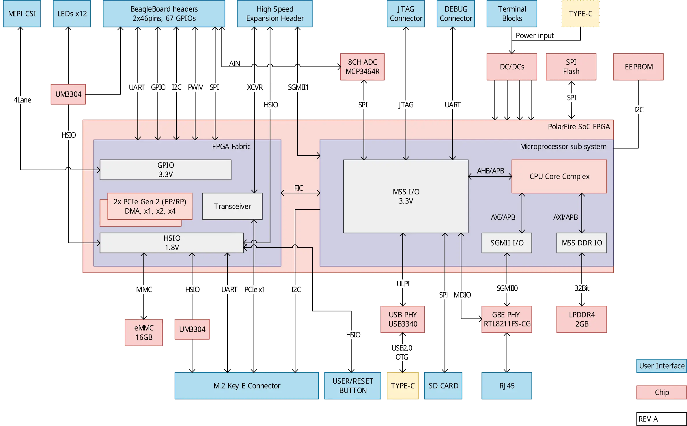
Fig. 231 System block diagram
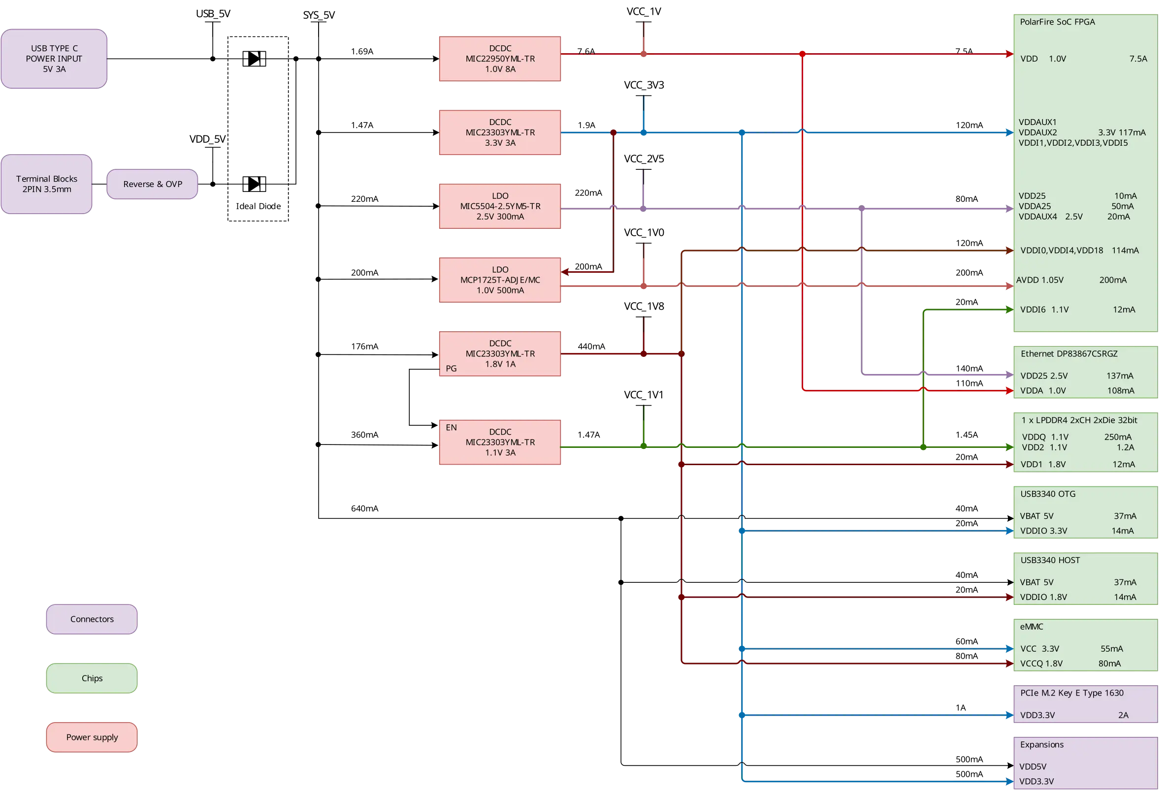
Fig. 232 Power tree diagram

Fig. 233 I2C tree diagram
System on Chip (SoC)
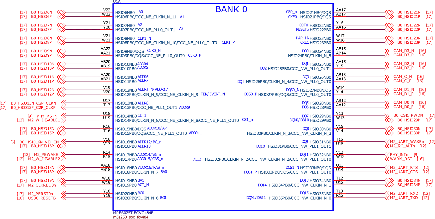
Fig. 234 SoC bank0
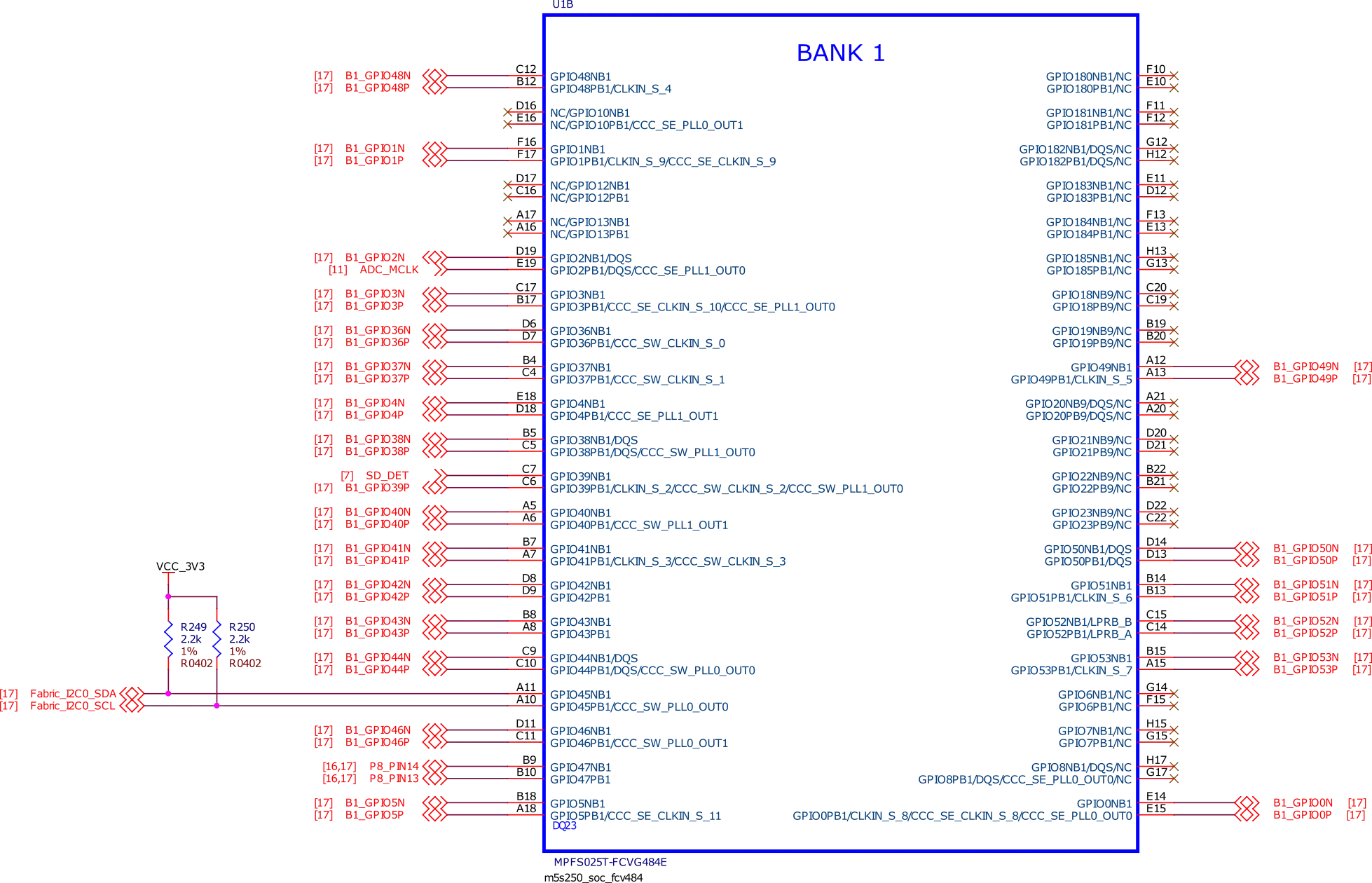
Fig. 235 SoC bank1
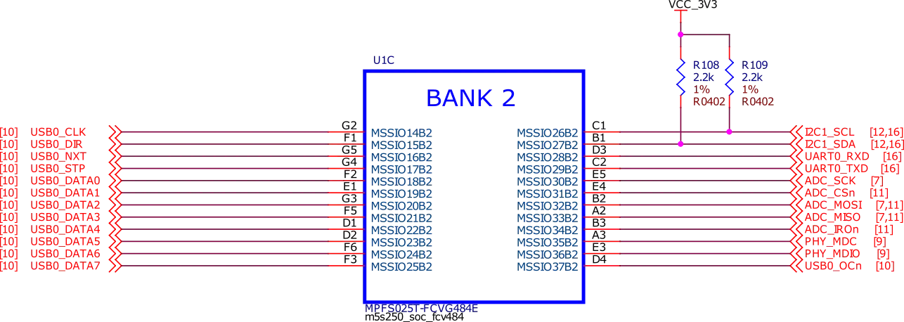
Fig. 236 SoC bank2
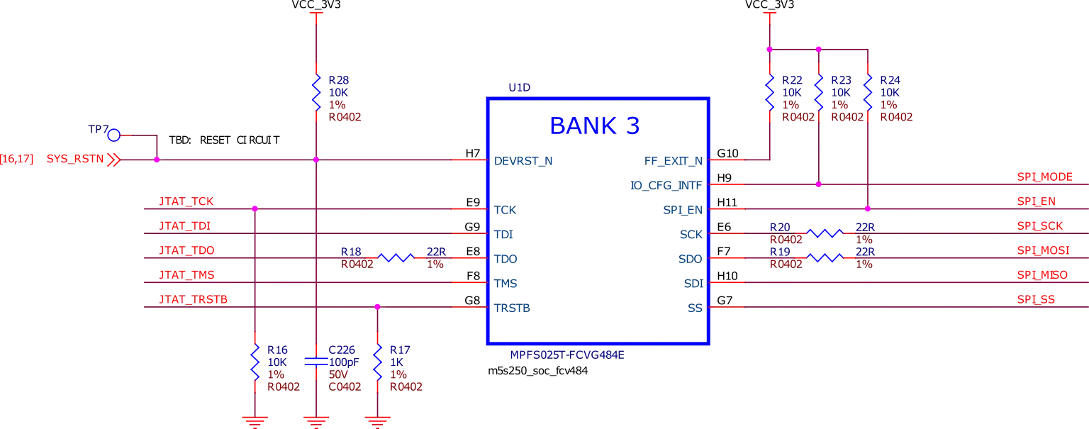
Fig. 237 SoC bank3
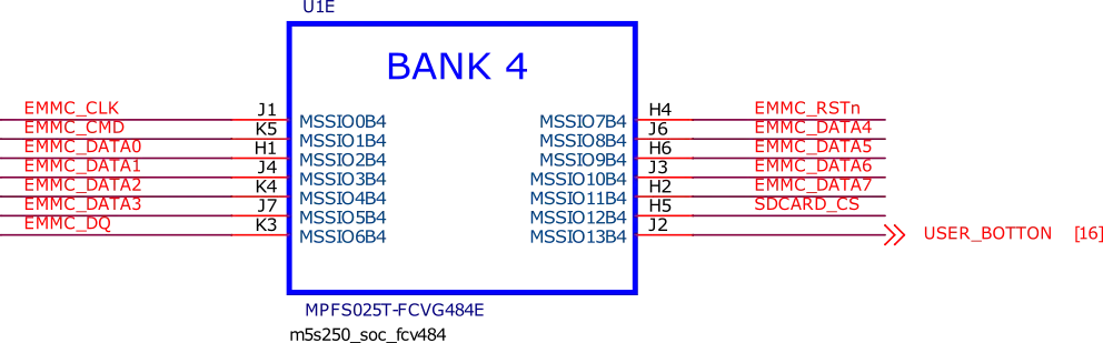
Fig. 238 SoC bank4
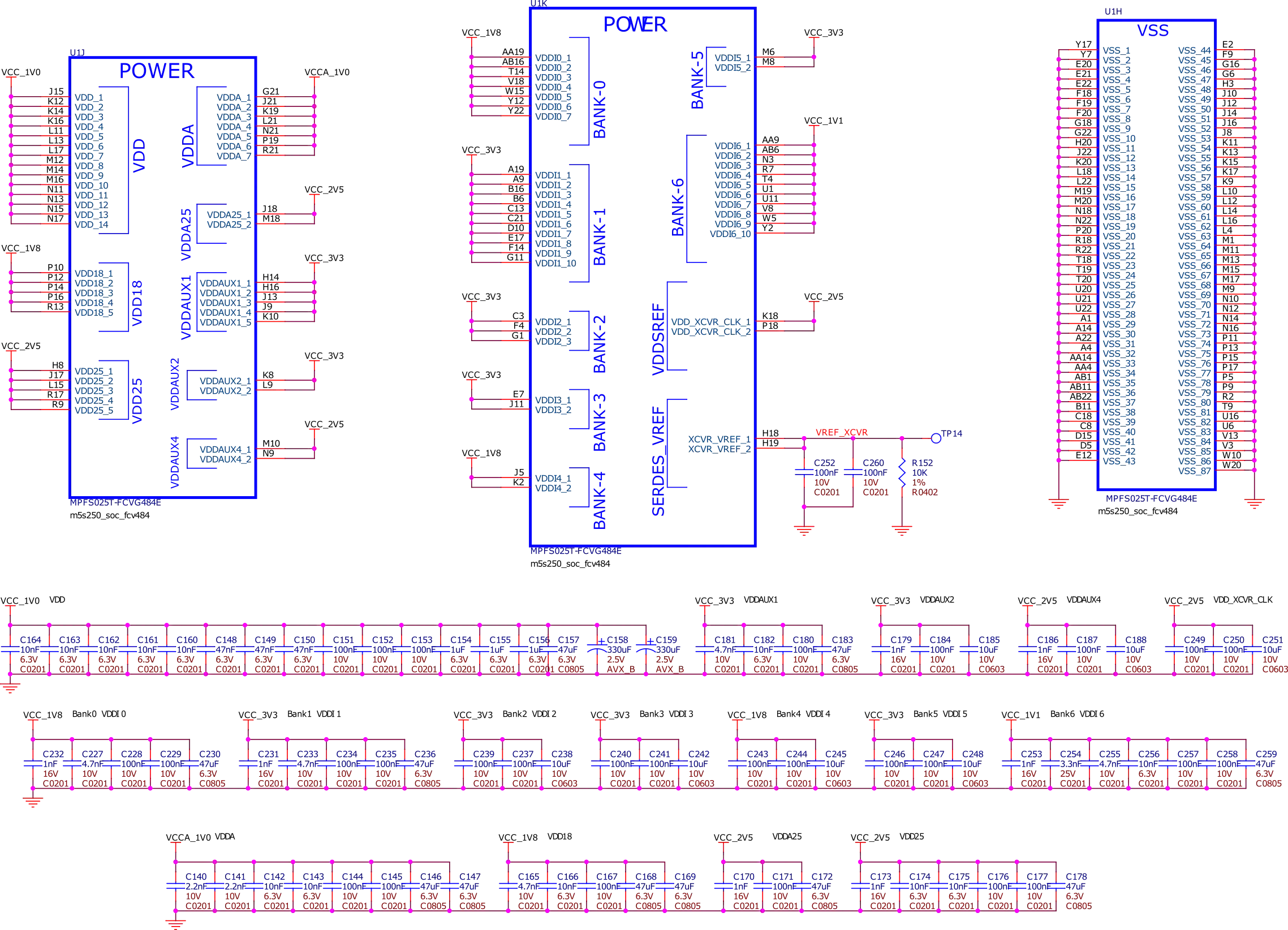
Fig. 239 SoC power
Power management
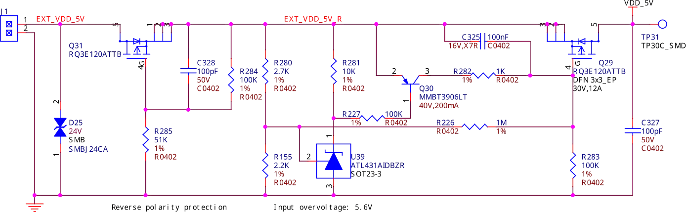
Fig. 240 DC 5V input
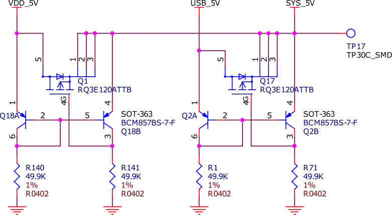
Fig. 241 Ideal diode
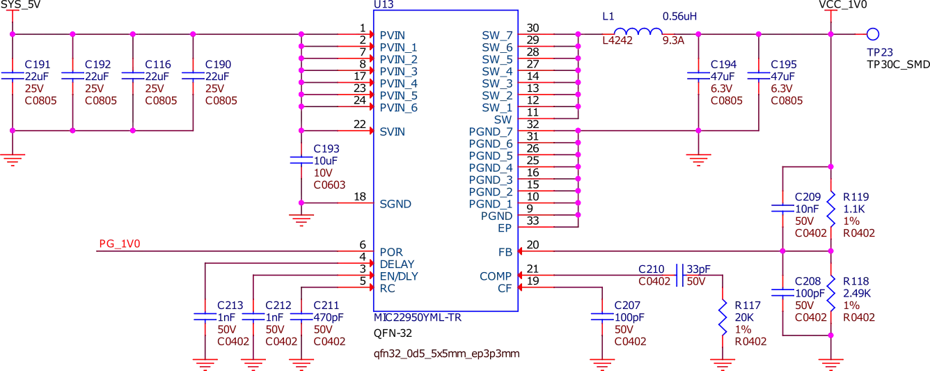
Fig. 242 VCC 1V0
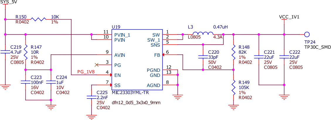
Fig. 243 VCC 1V1
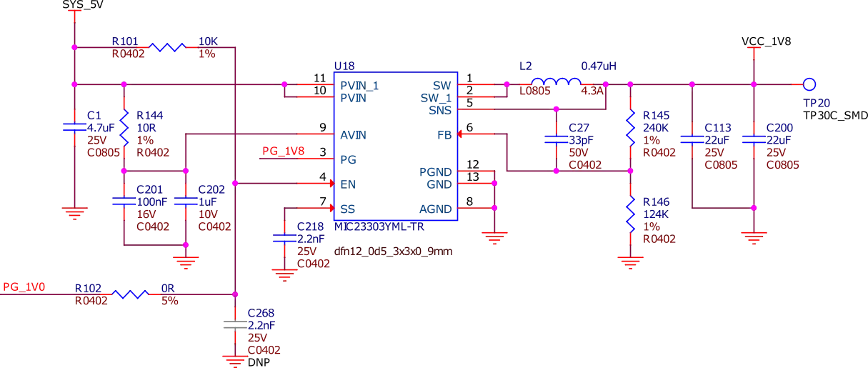
Fig. 244 VCC 1V8
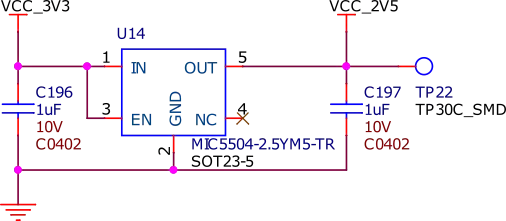
Fig. 245 VCC 2V5
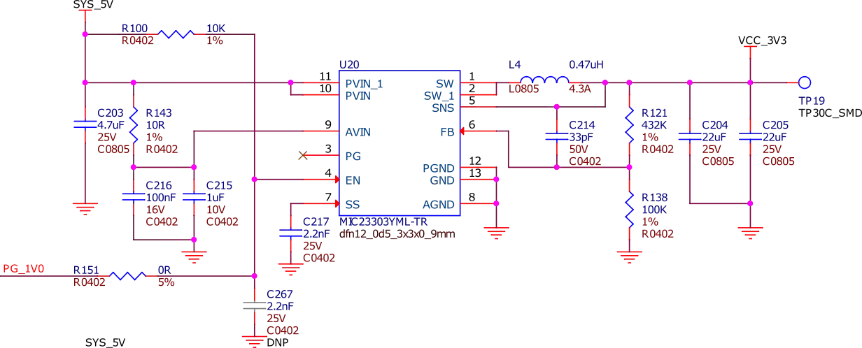
Fig. 246 VCC 3V3
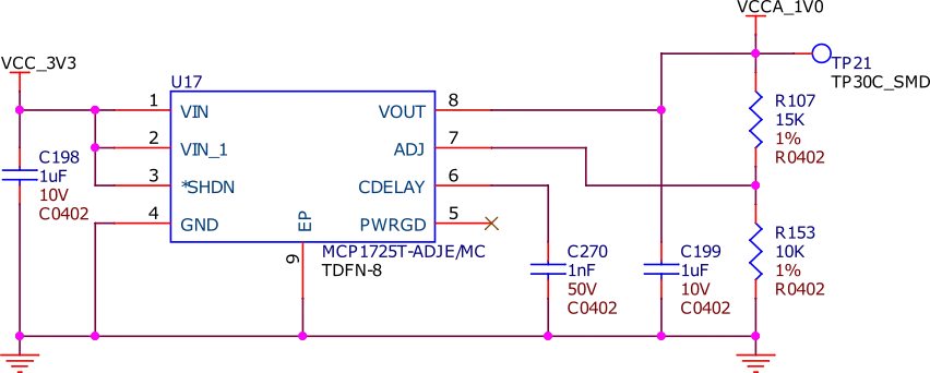
Fig. 247 VCCA 1V0
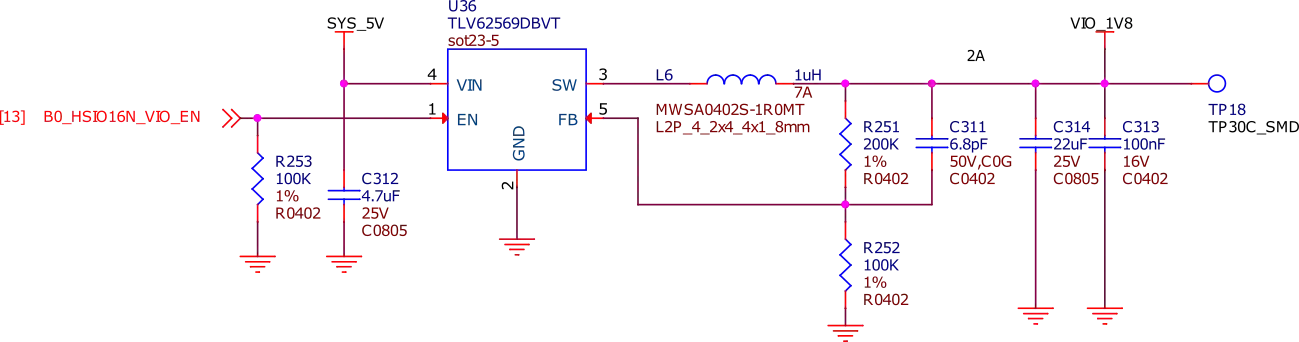
Fig. 248 VIO enable
General Connectivity and Expansion
USB-C port
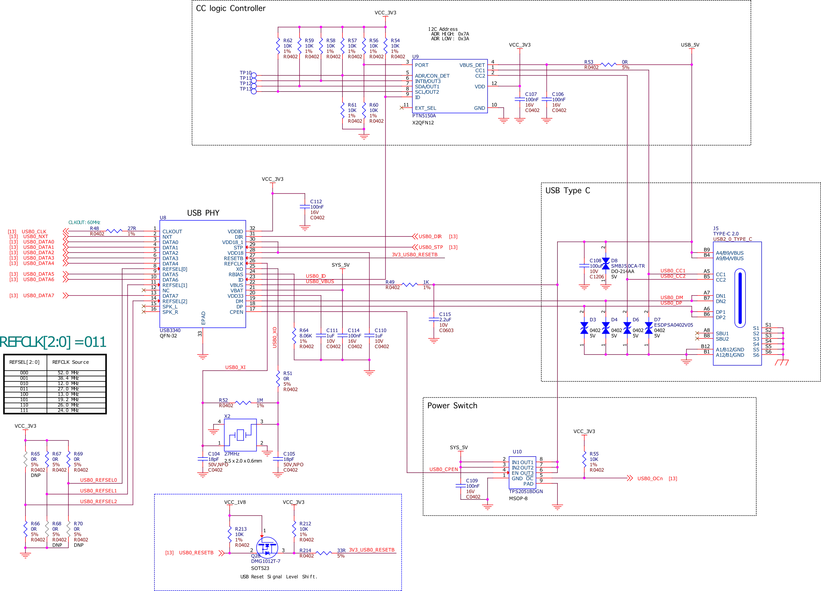
Fig. 249 USB C
P8 & P9 cape header pins
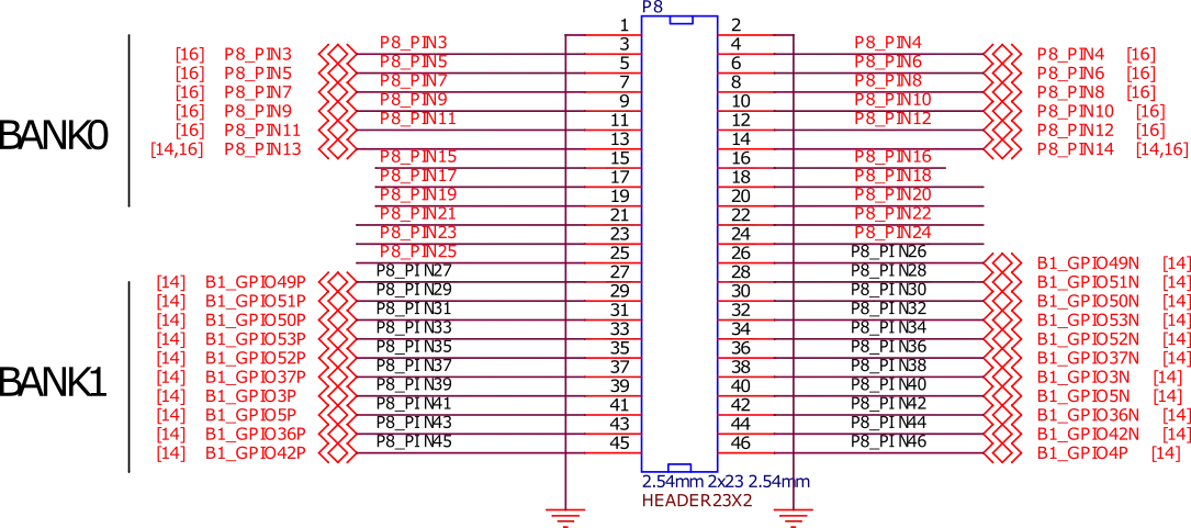
Fig. 250 P8 cape header
Fig. 251 P9 cape header
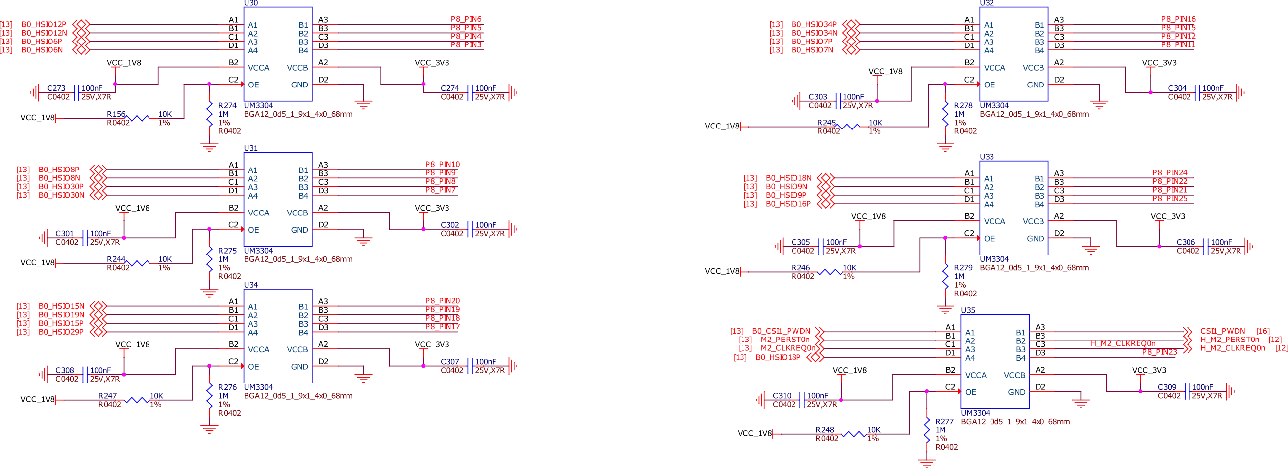
Fig. 252 Cape header voltage level translator
ADC
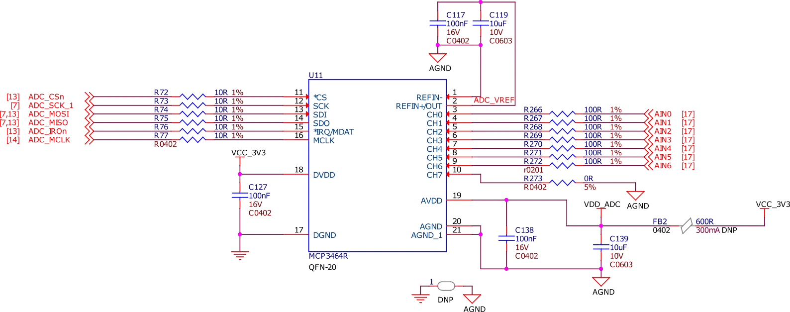
Fig. 253 16bit Delta-Sigma ADC
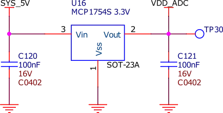
Fig. 254 ADC LDO power supply
Buttons and LEDs
User LEDs and Power LED
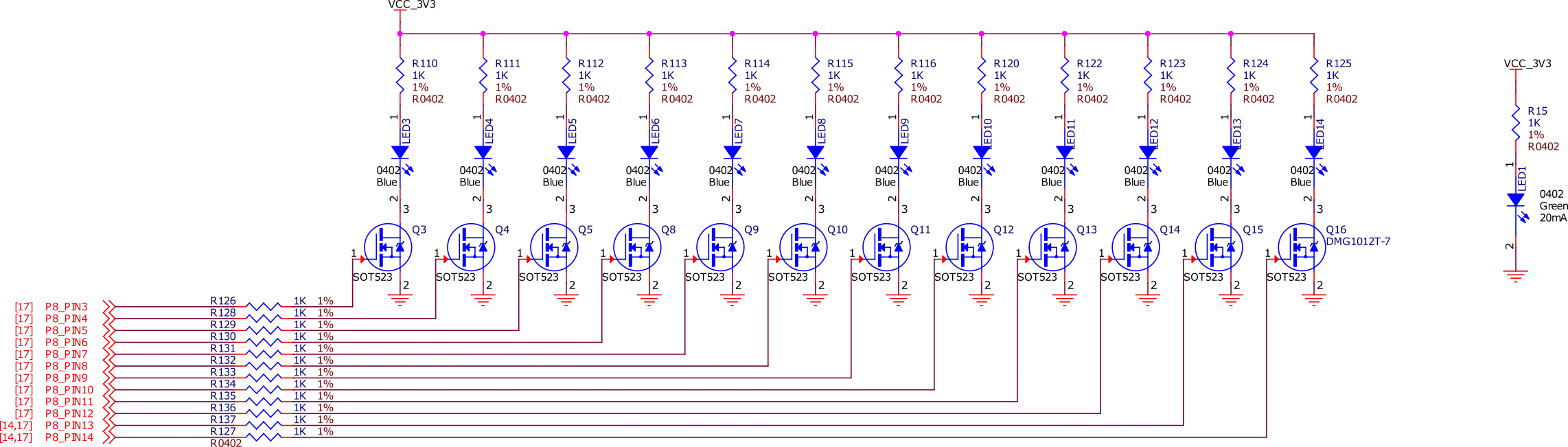
Fig. 255 User LEDs and power LED
User and reset button
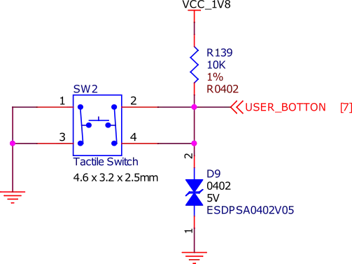
Fig. 256 User button
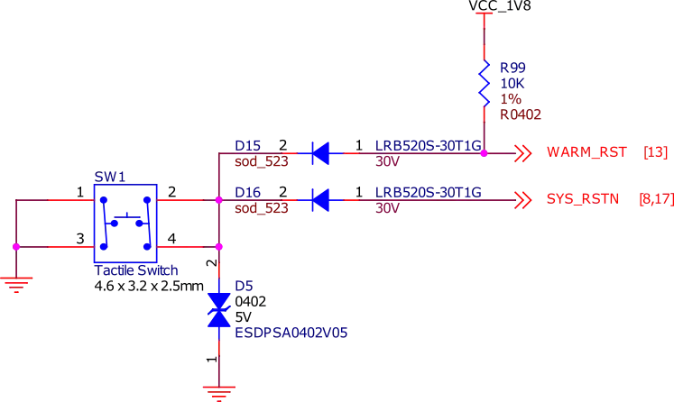
Fig. 257 Reset button
Connectivity
Ethernet
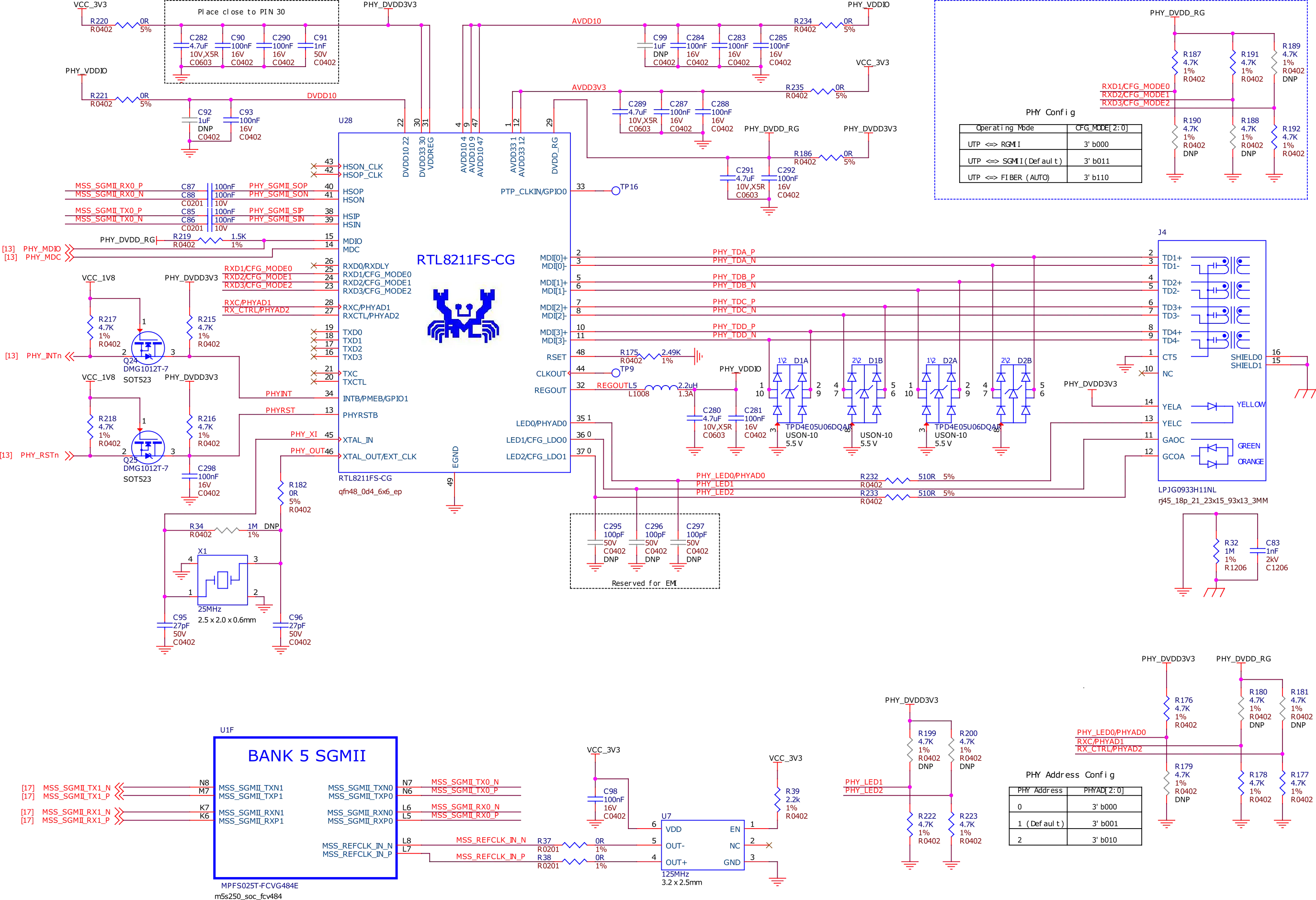
Fig. 258 Gigabit ethernet
Memory, Media and Data storage
DDR memory
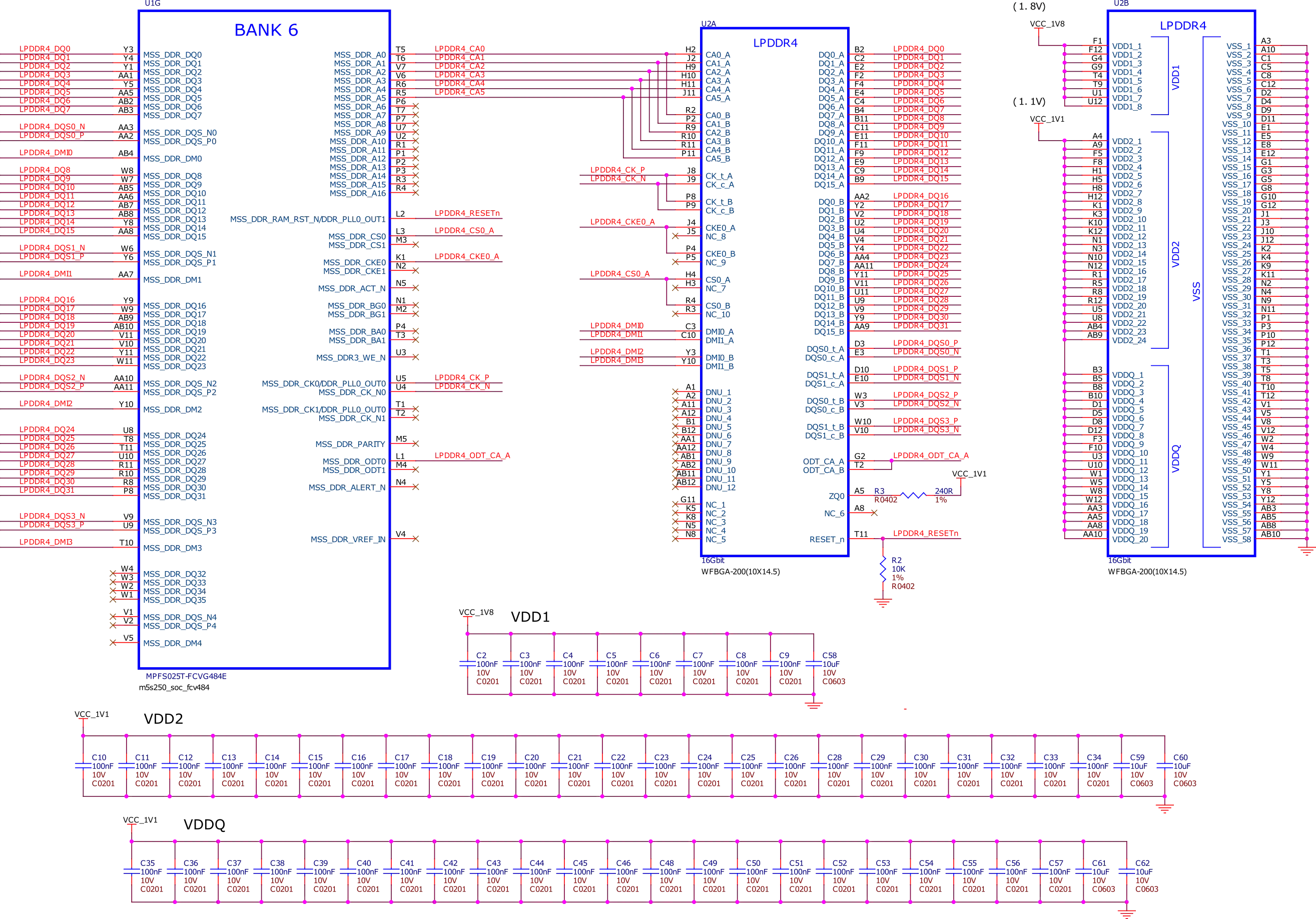
Fig. 259 LPDDR memory
eMMC
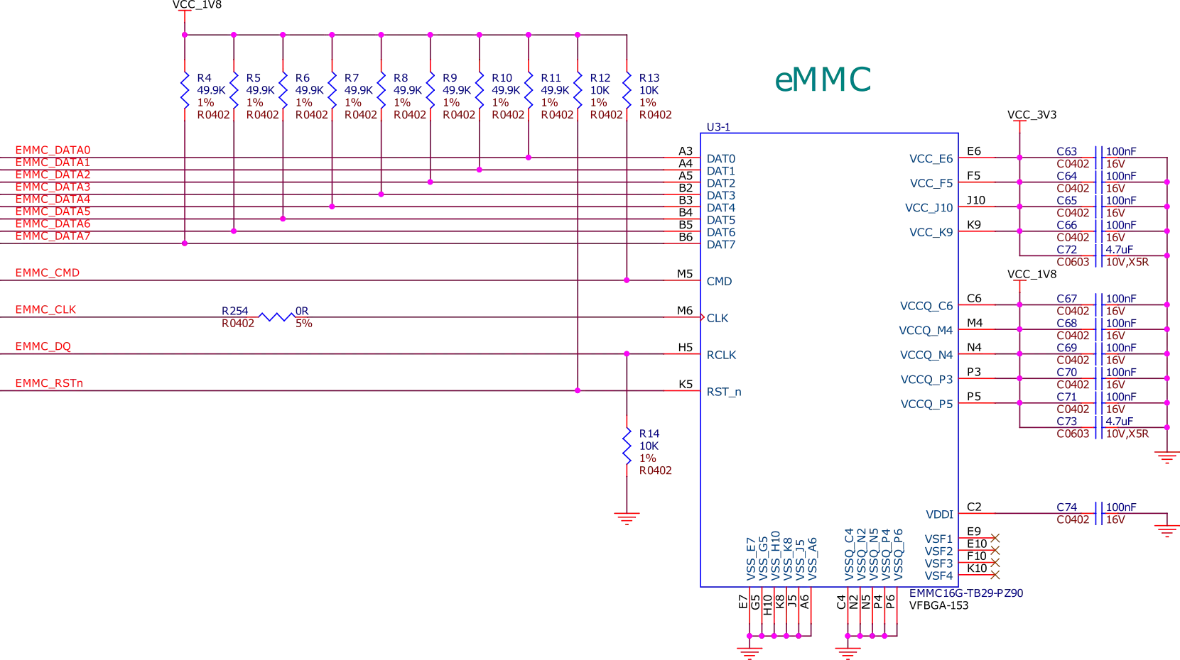
Fig. 260 EMMC flash storage
microSD
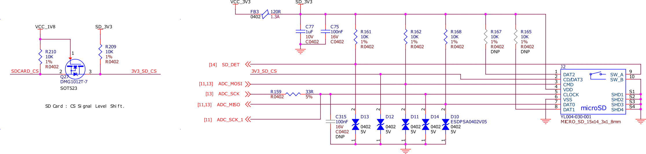
Fig. 261 SD Card socket
EEPROM
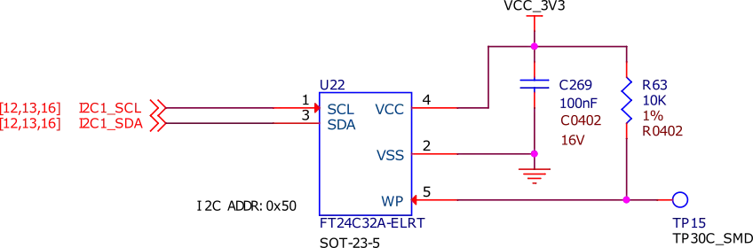
Fig. 262 EEPROM
SPI flash
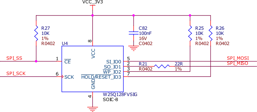
Fig. 263 SPI Flash
Multimedia I/O
CSI
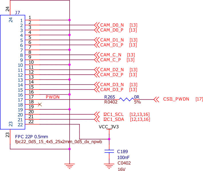
Fig. 264 CSI
Debug
UART debug port
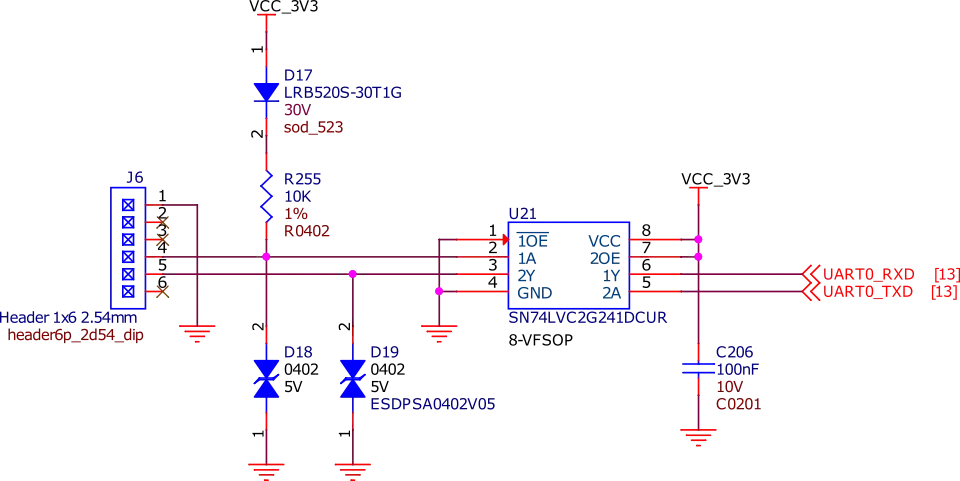
Fig. 265 UART debug header
JTAG debug port
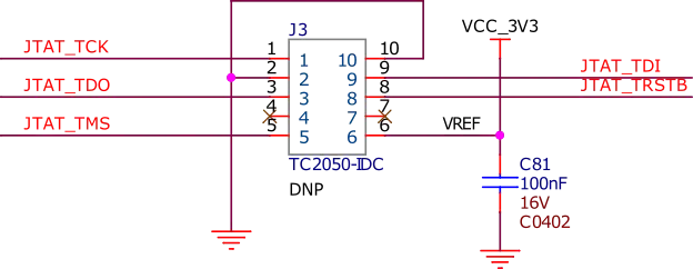
Fig. 266 JTAG debug header
Mechanical Specifications
Parameter |
Values |
|---|---|
Size |
86.38 * 54.61 * 18.8 mm |
Max heigh |
18.8 mm |
PCB Size |
86.38 * 54.6 mm |
PCB Layers |
12 Layers |
PCB Thickness |
1.6 mm |
RoHS compliant |
Yes |
Gross Weight |
106 g |
Net weight |
45.8 g |