Design & specifications
If you want to know how BeagleV Ahead board is designed and what are it’s high-level specifications then this chapter is for you. We are going to discuss each hardware design element in detail and provide high-level device specifications in a short and crisp form as well.
Block diagram
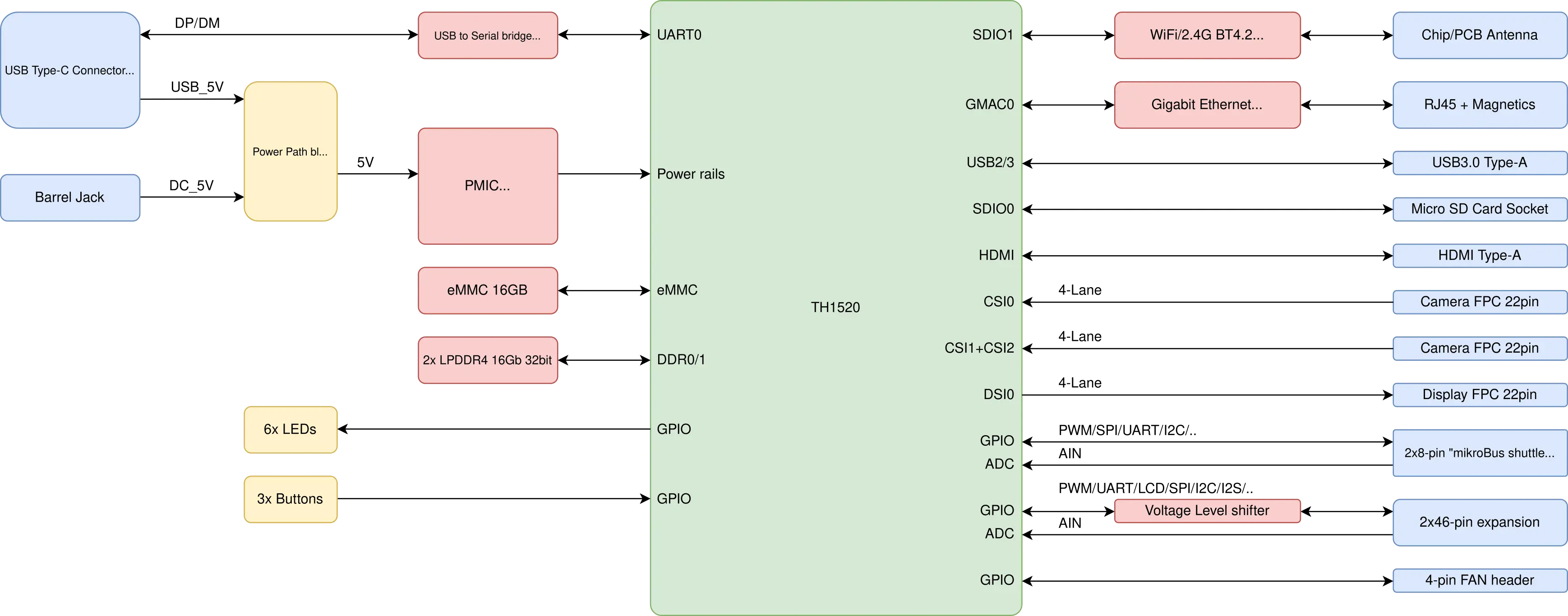
Fig. 190 System block diagram
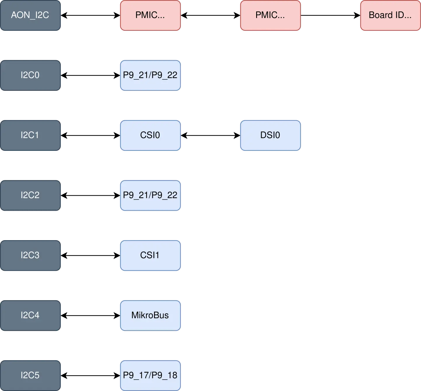
Fig. 191 I2C-Usage diagram
System on Chip (SoC)
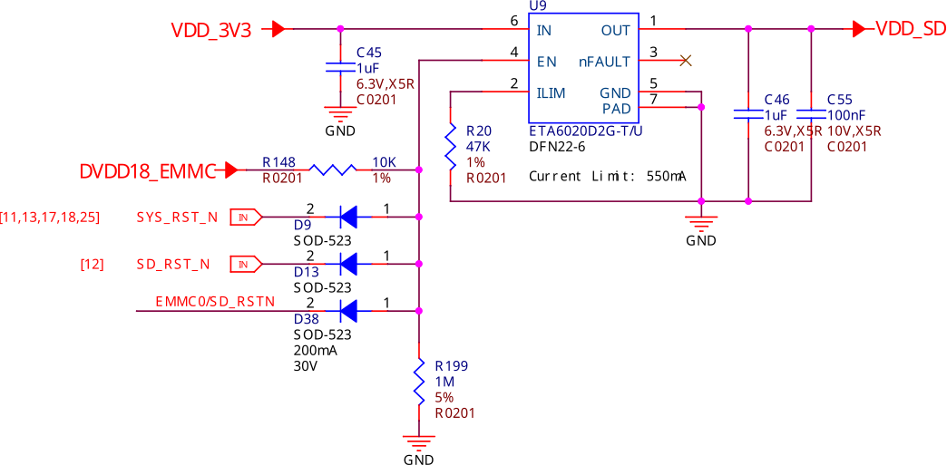
Fig. 192 SoC eMMC power switch
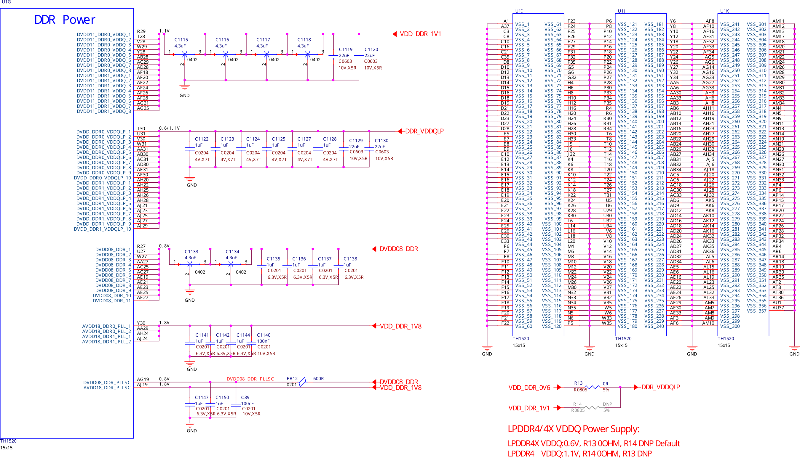
Fig. 193 SoC DDR Power
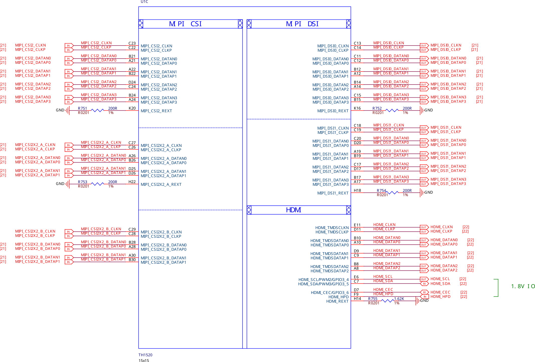
Fig. 194 SoC MIPI CSI DSI HDMI
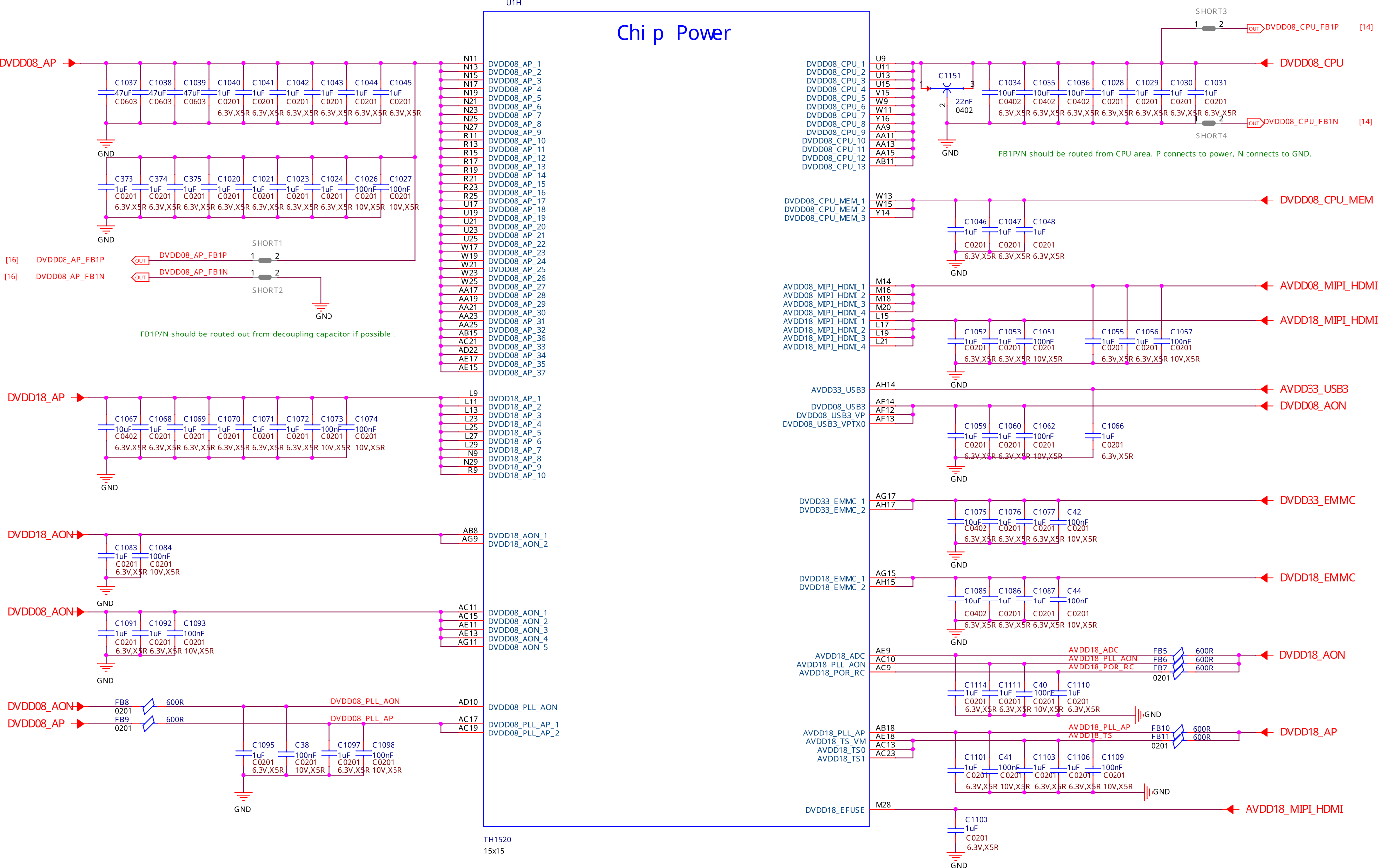
Fig. 195 SoC power
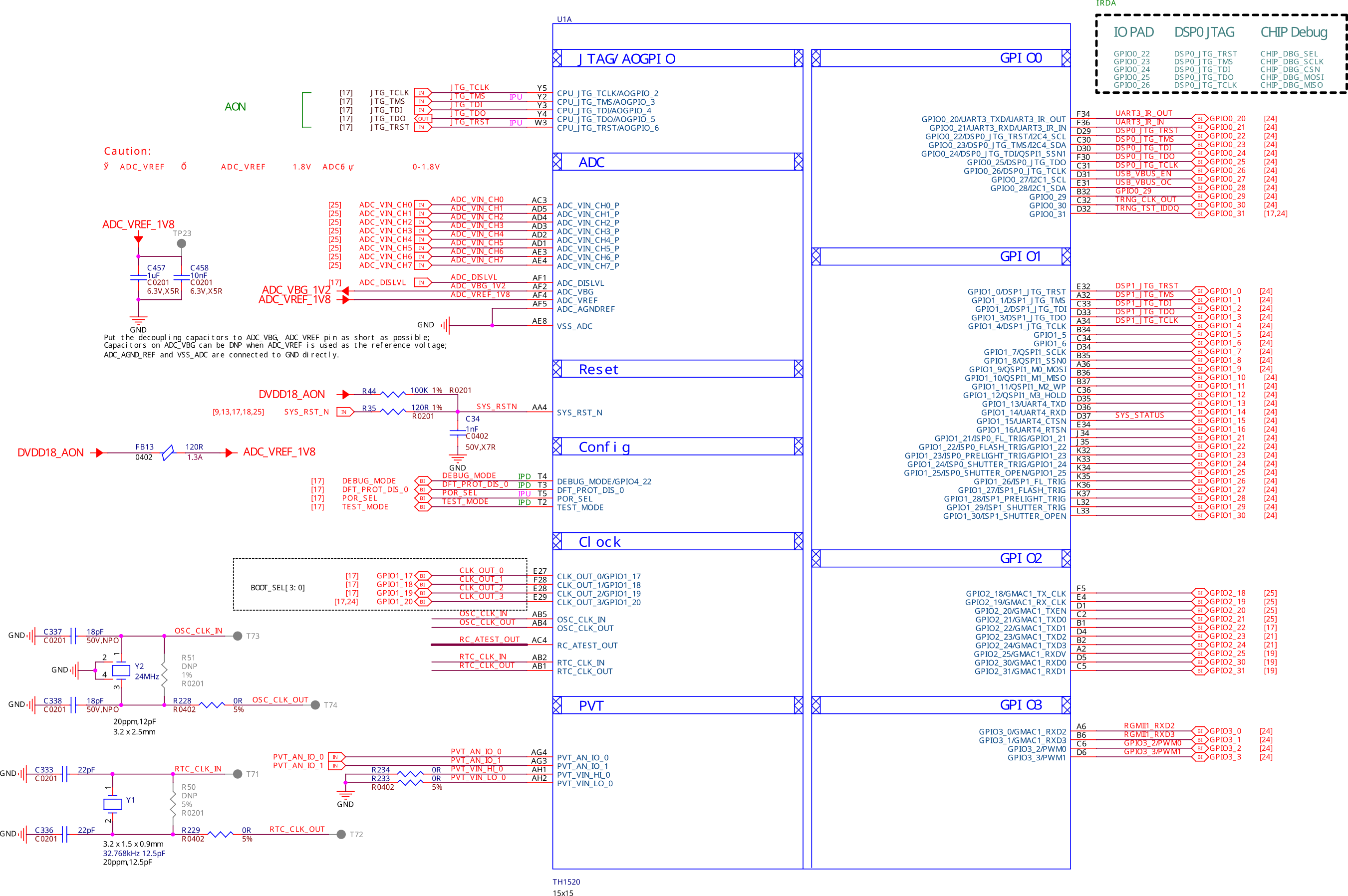
Fig. 196 SoC sys, ADC, and Clock
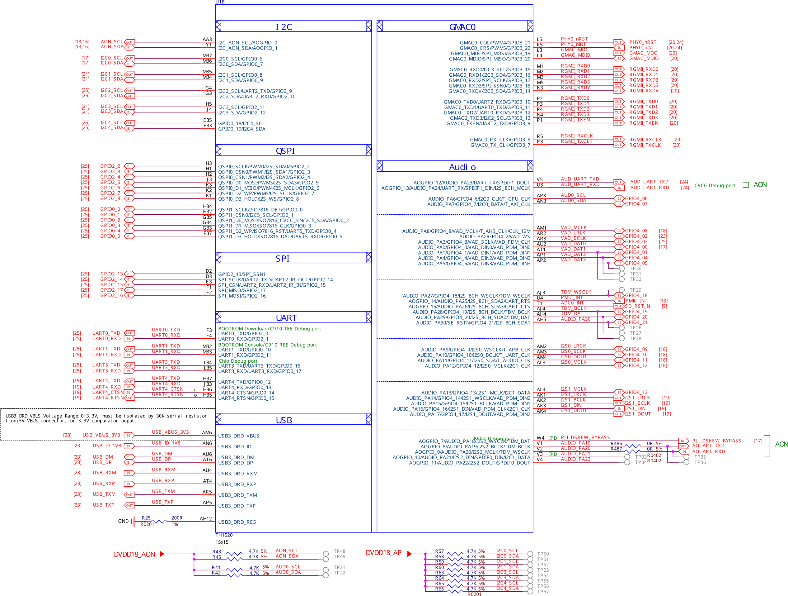
Fig. 197 SoC USB GMAC Audio
Power management
Barrel jack
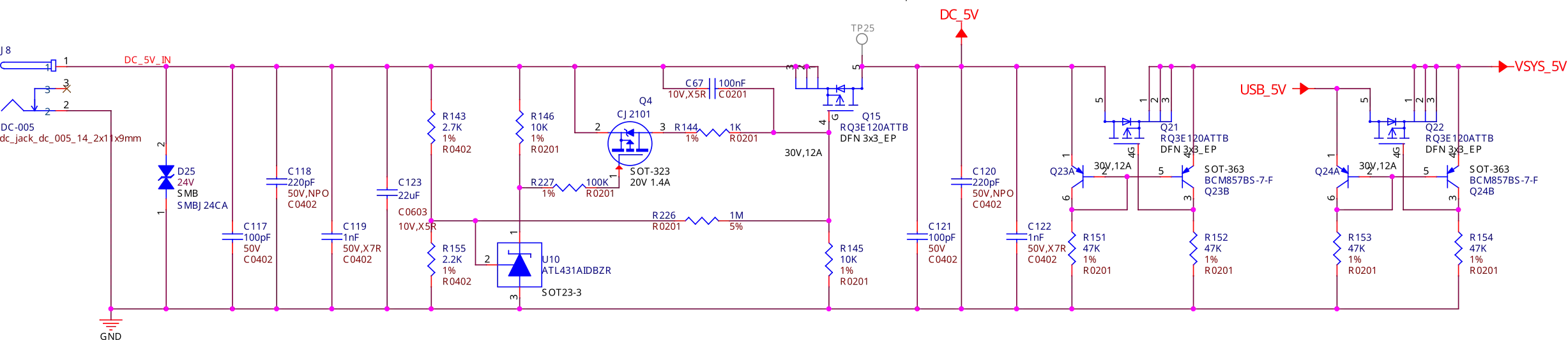
Fig. 198 Barrel jack power input
0.8V DCDC buck
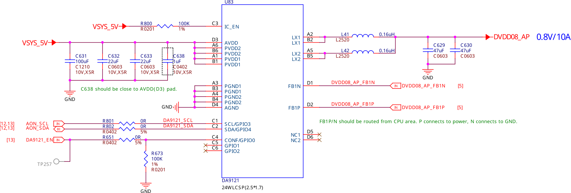
Fig. 199 0.8V DCDC buck converter
3.3V DCDC buck
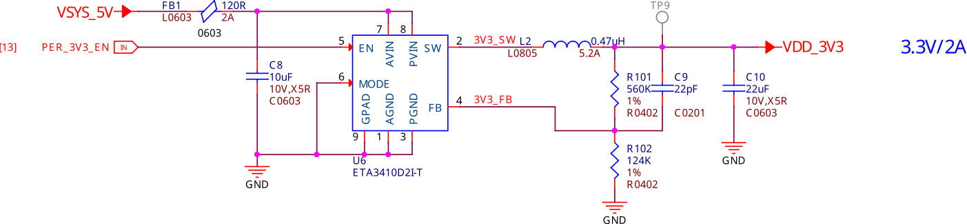
Fig. 200 3.3V DCDC buck converter
1.8V LDO
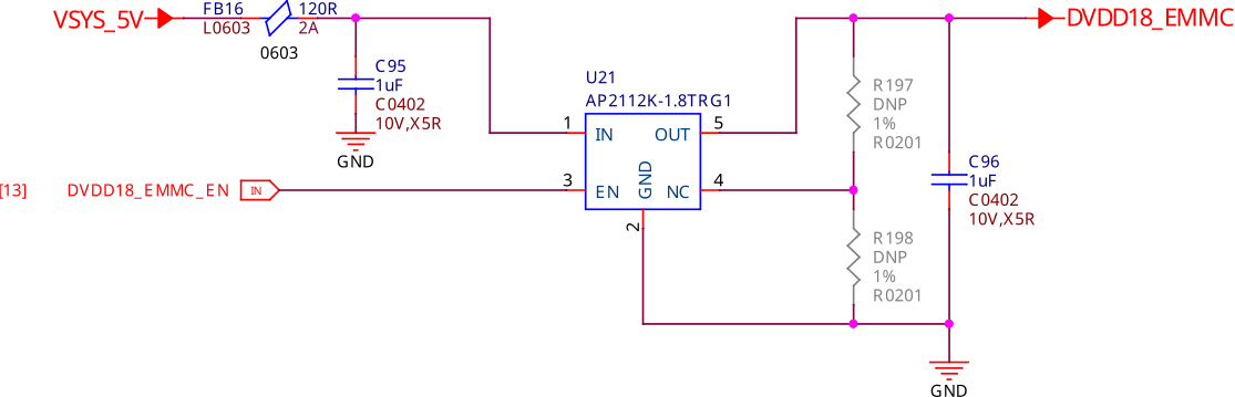
Fig. 201 1.8V LDO regulator
PMIC
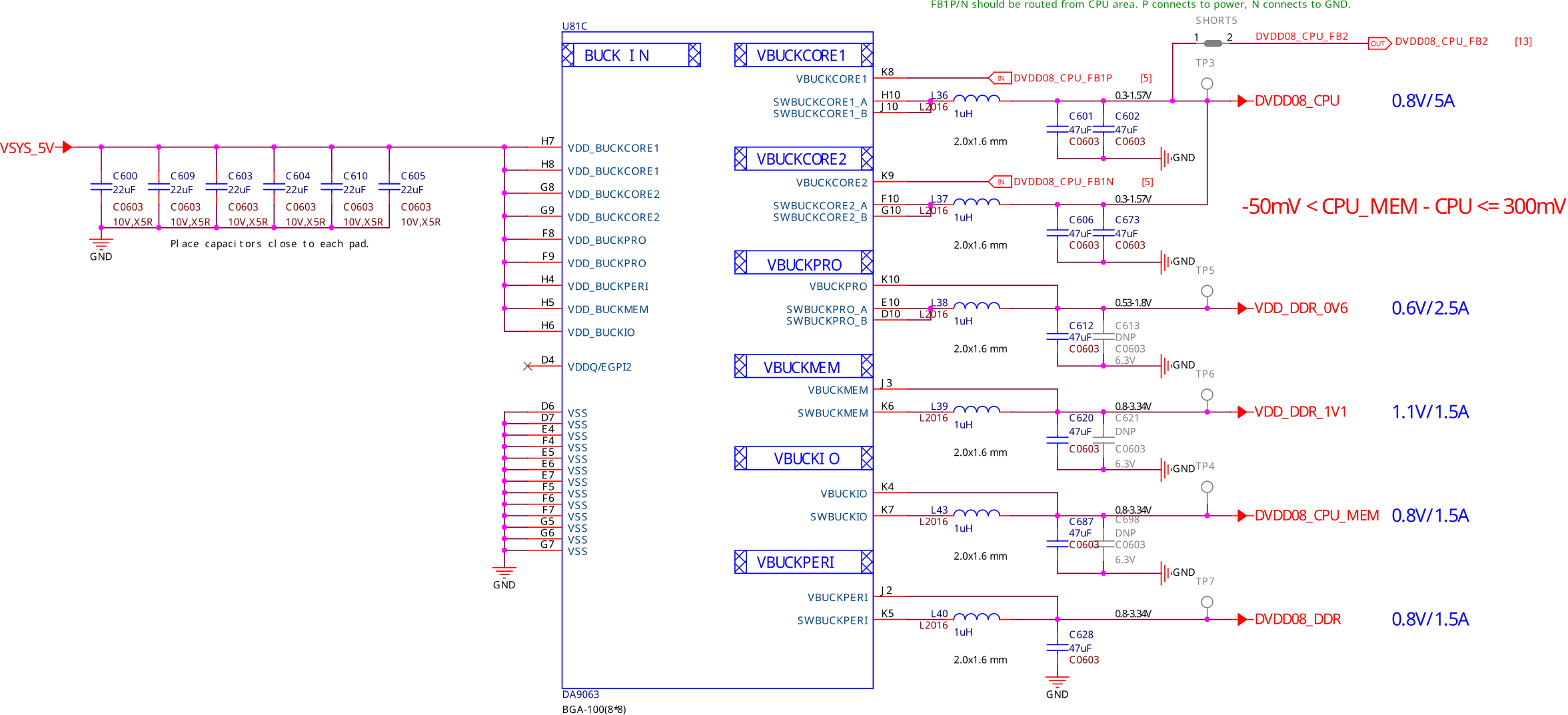
Fig. 202 PMIC Buck
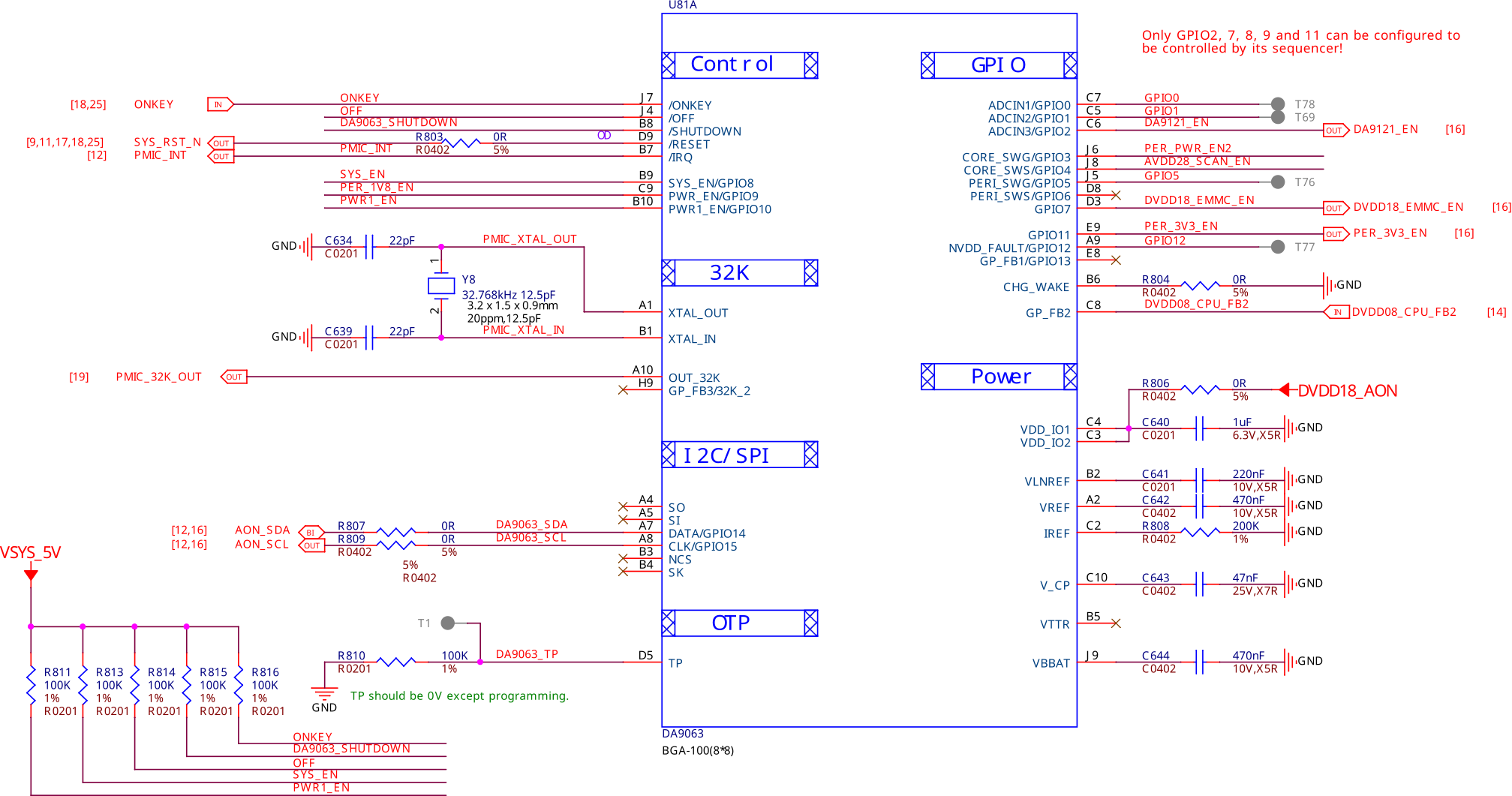
Fig. 203 PMIC Control
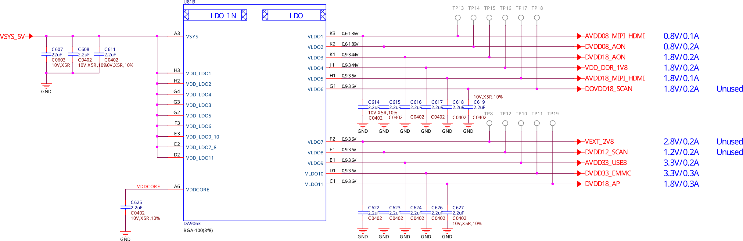
Fig. 204 PMIC LDO
General Connectivity and Expansion
microUSB 3.0 port
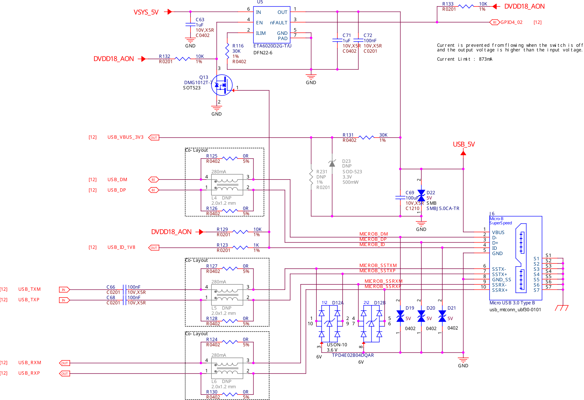
Fig. 205 microUSB 3.0 port
P8 & P9 cape header pins
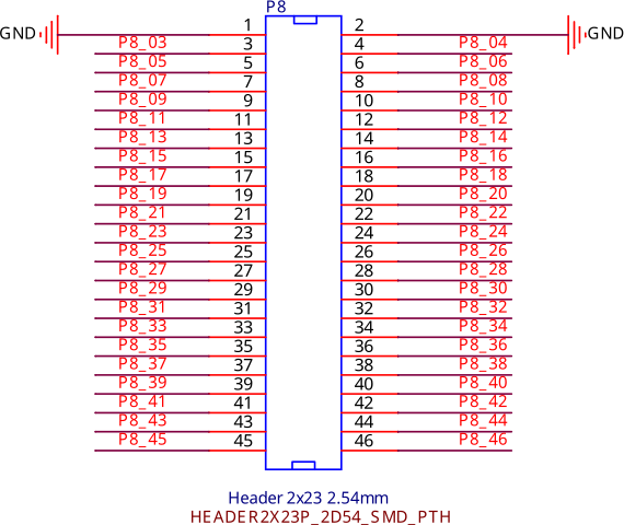
Fig. 206 P8 cape header
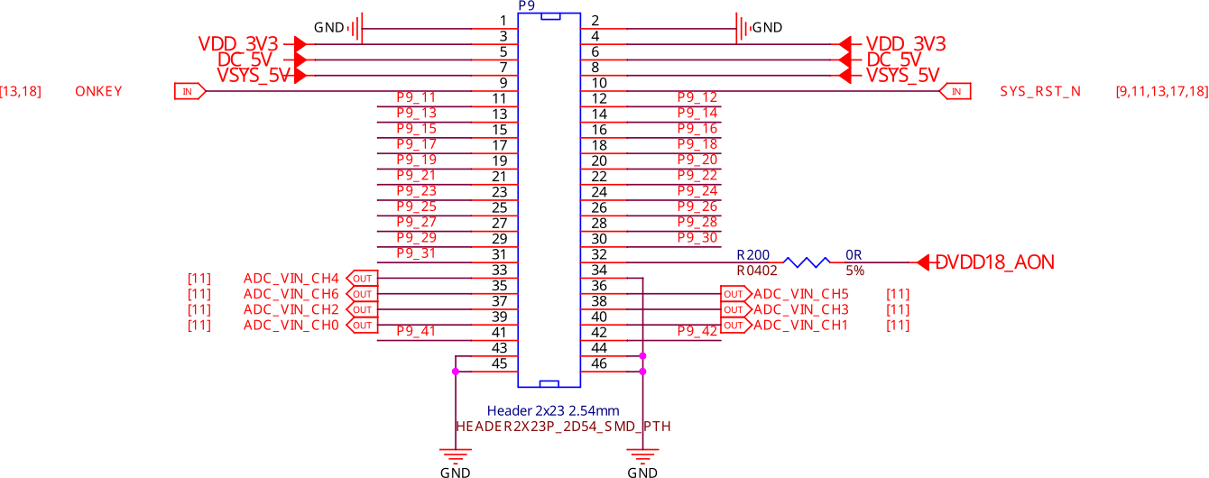
Fig. 207 P9 cape header
mikroBUS shuttle connector
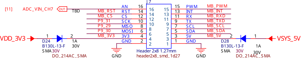
P8, P9, and mikroBUS helper circuitry
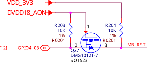
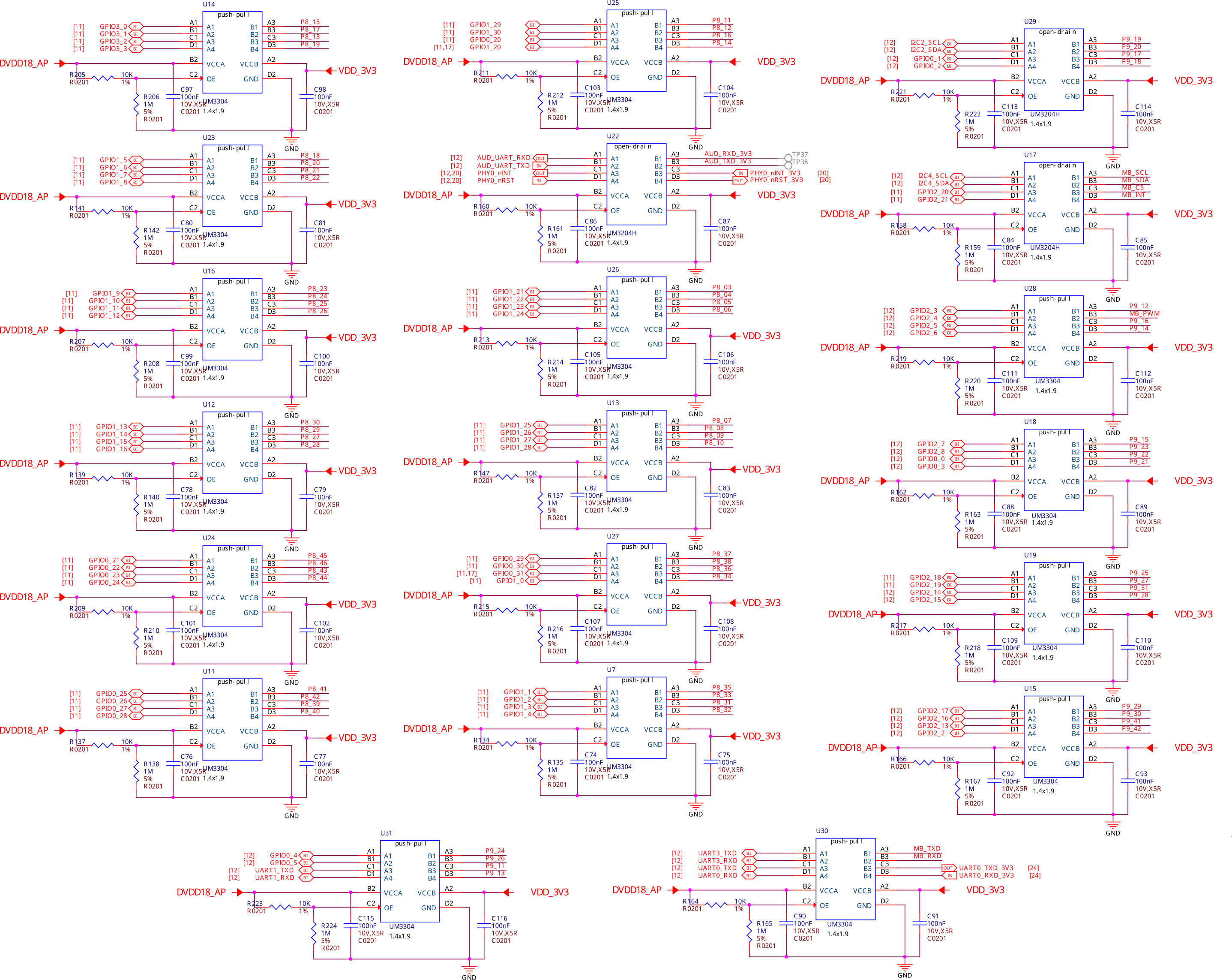
Fig. 208 P8, P9, and mikroBUS level shifters
Buttons and LEDs
Boot select buttons
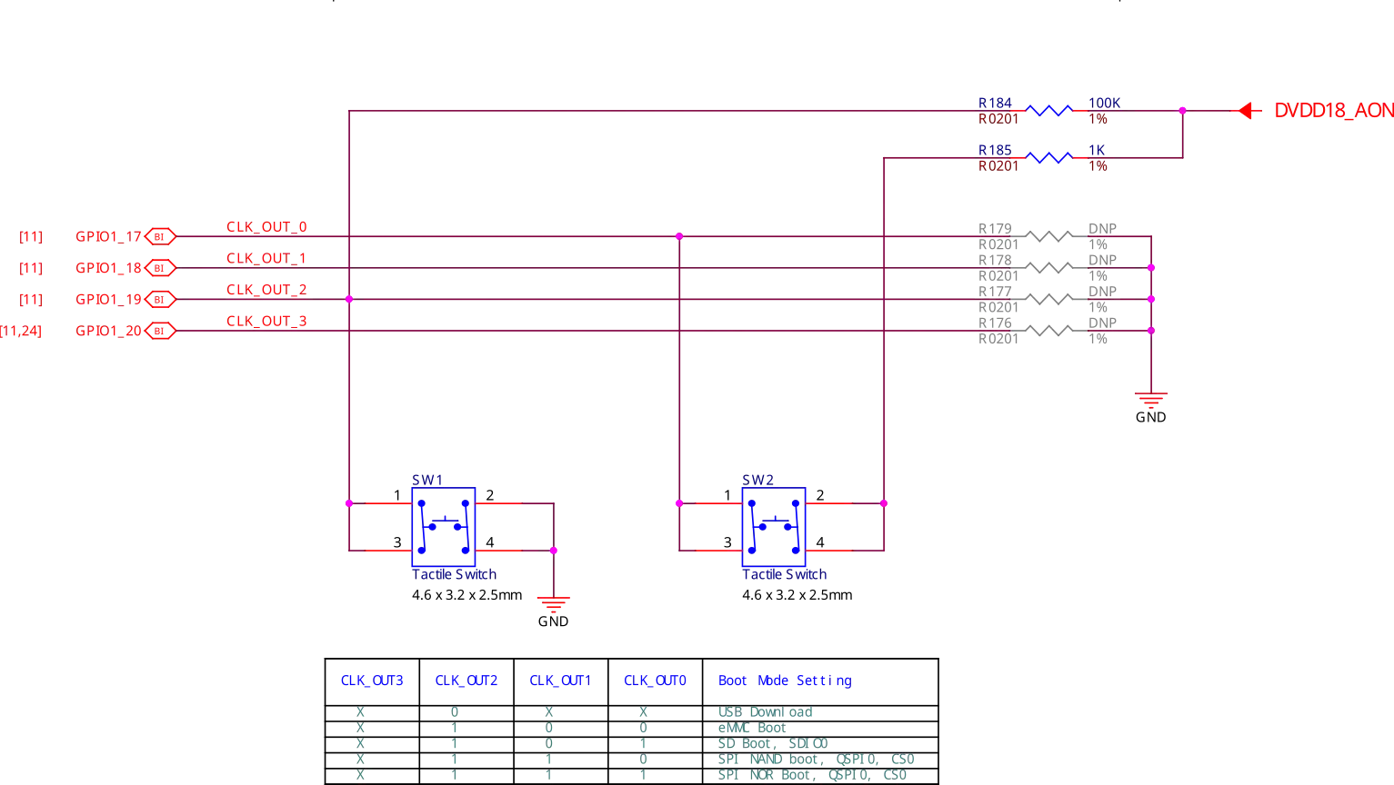
Fig. 209 Boot select buttons
User LEDs and Power LED
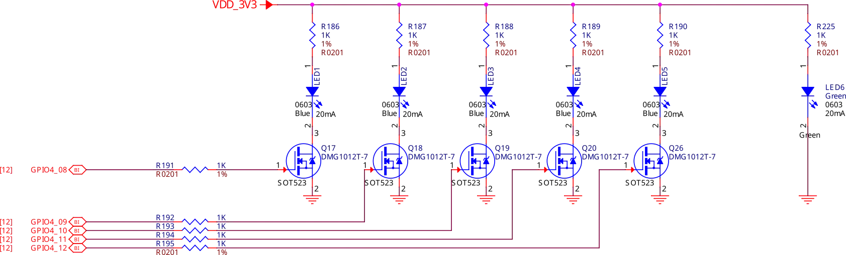
Fig. 210 User LEDs and power LED
Power and reset button
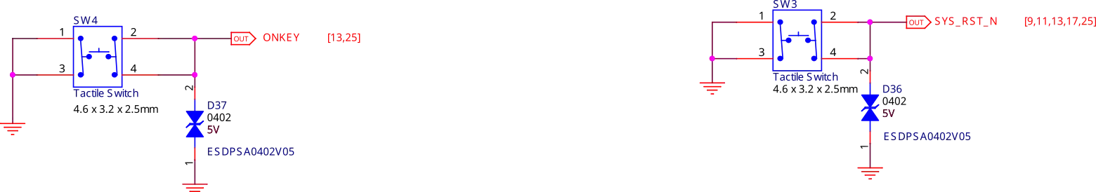
Fig. 211 Power and reset button
Wired and wireless connectivity
Ethernet
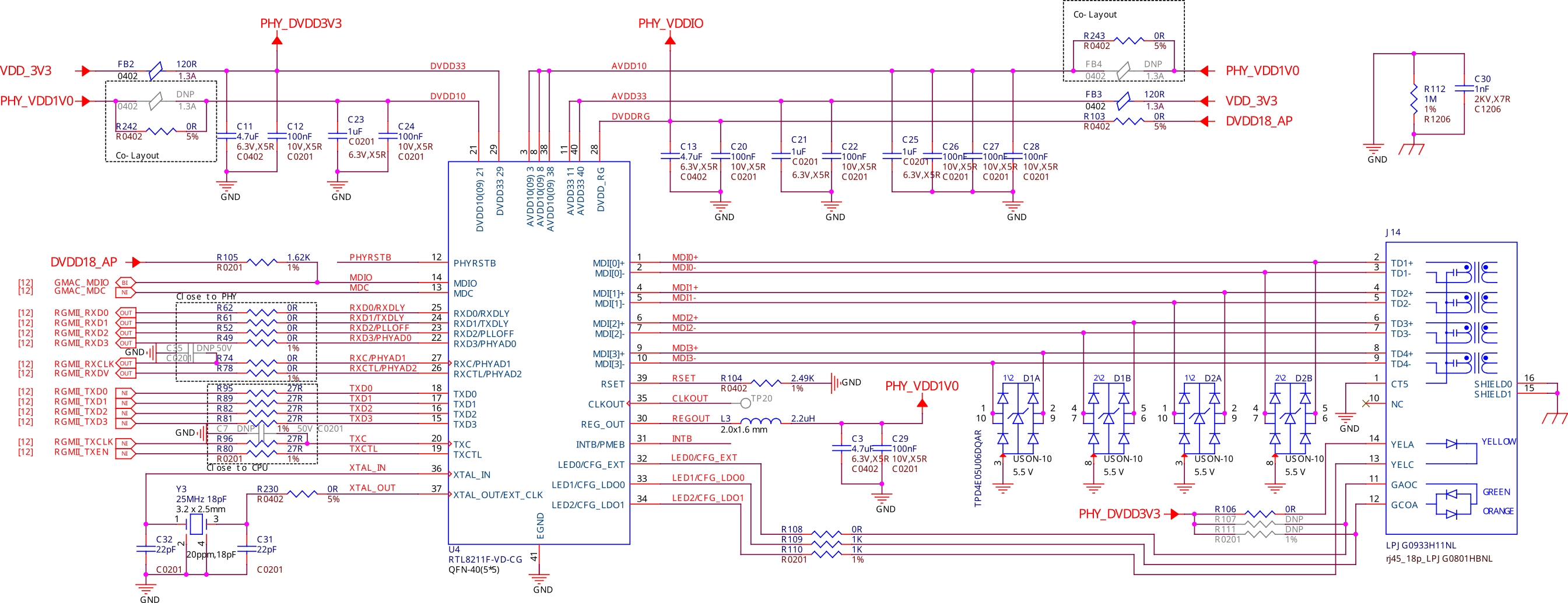
Fig. 212 Ethernet
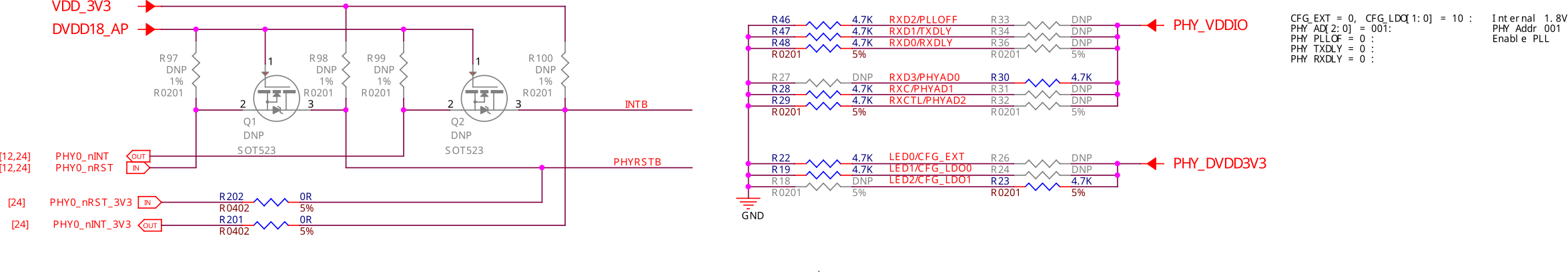
Fig. 213 Ethernet LevelShifter and Strapping
WiFi & Bluetooth
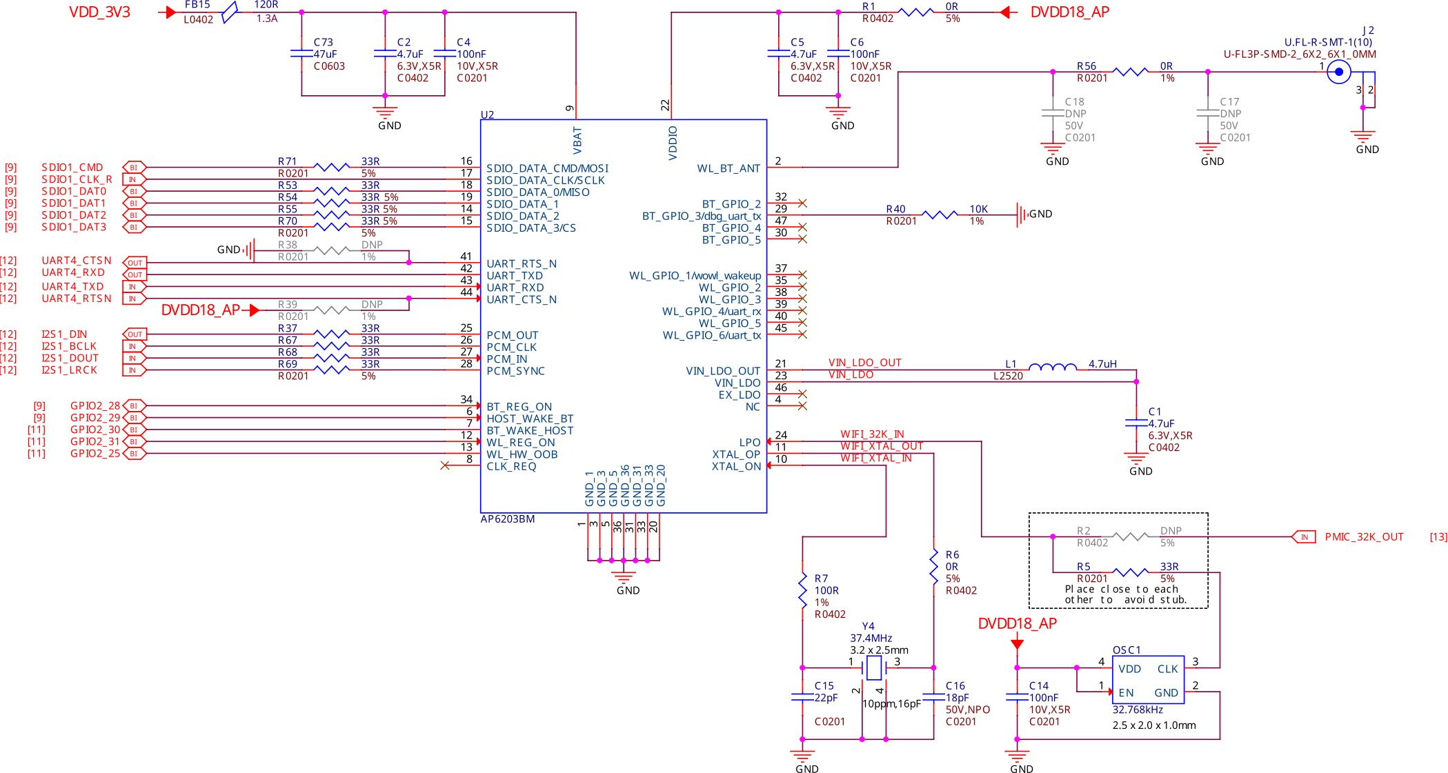
Fig. 214 WiFi and Bluetooth
Memory, Media and Data storage
DDR memory
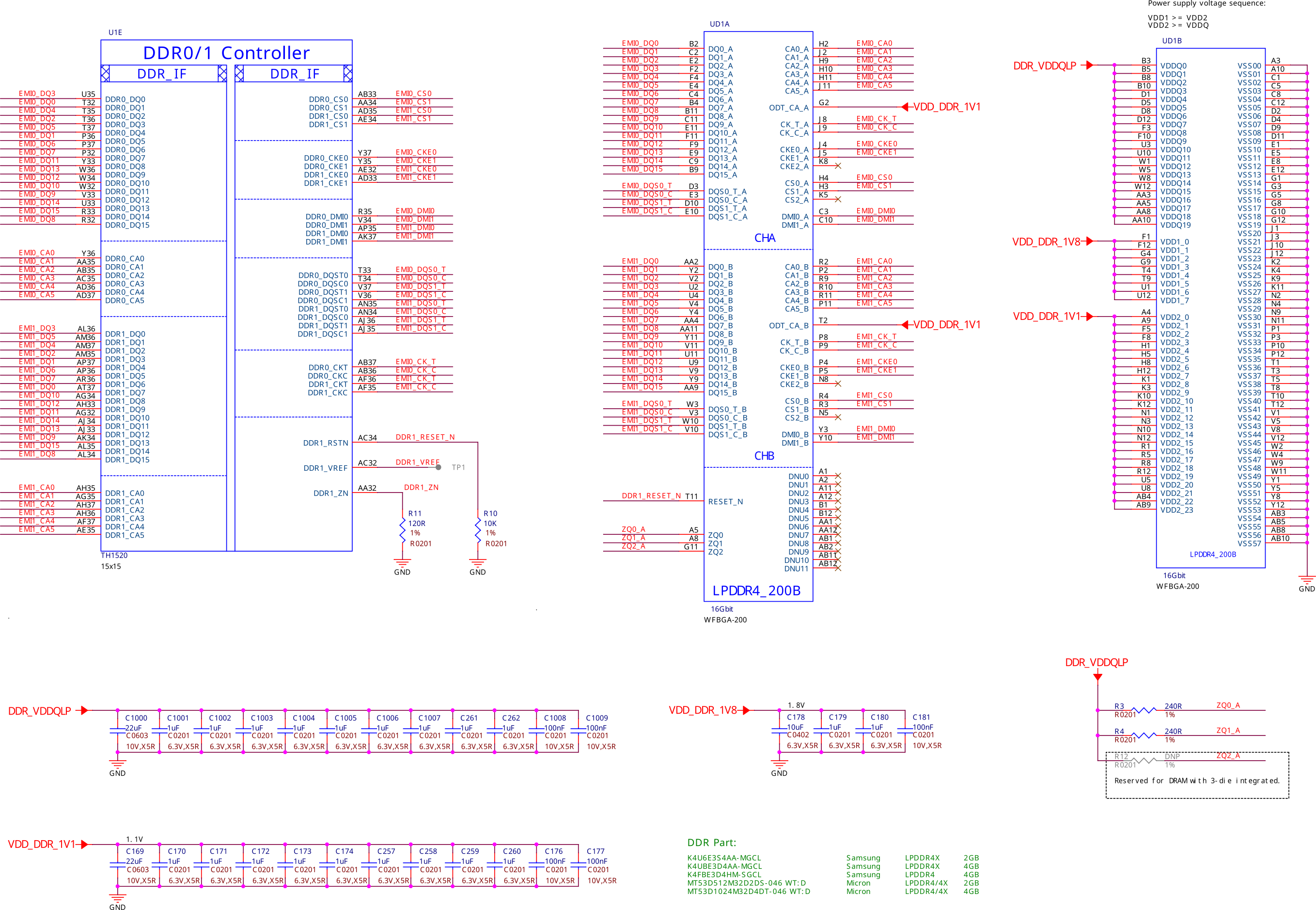
Fig. 215 2GB DDR4 Memory chip1
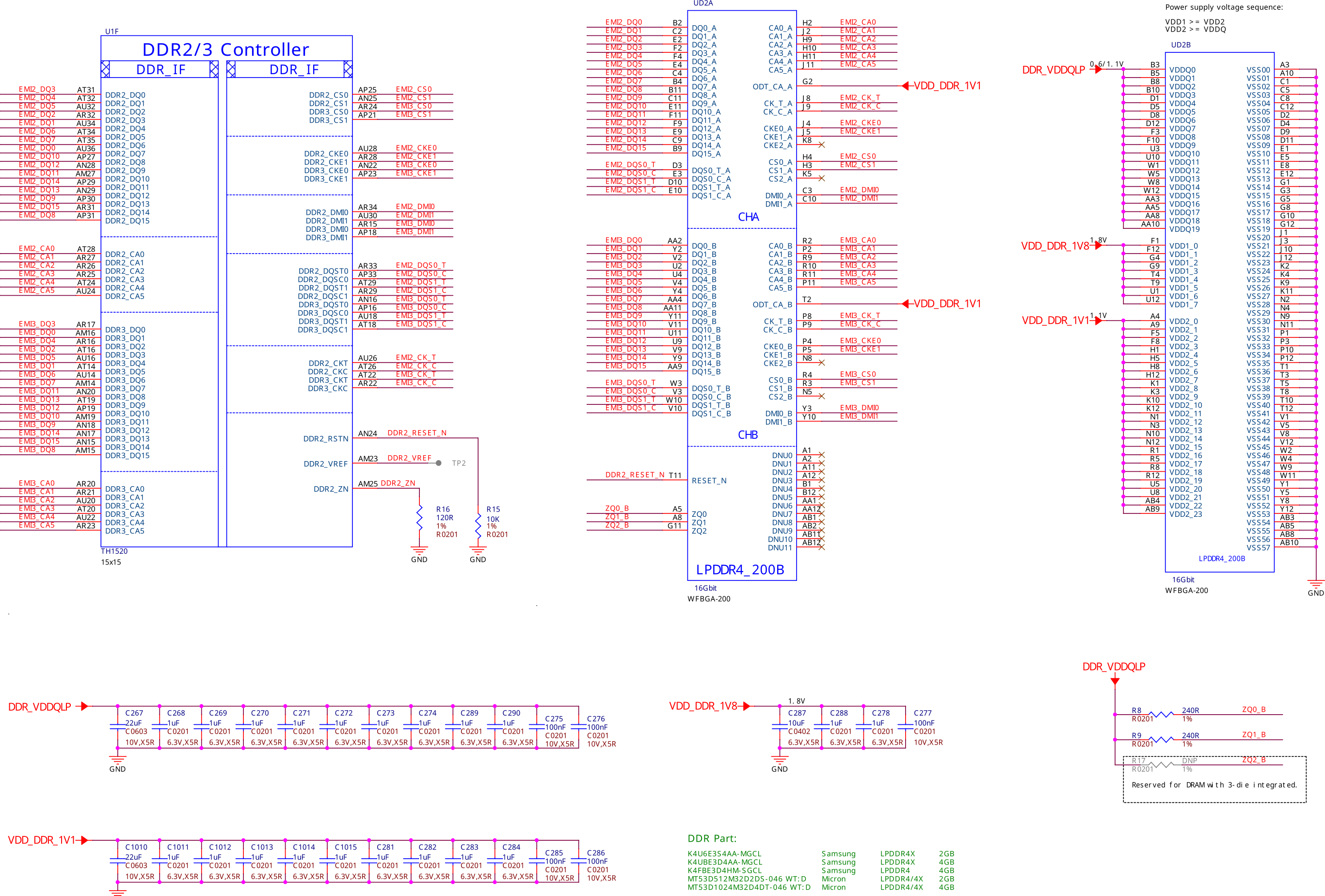
Fig. 216 2GB DDR4 Memory chip2
eMMC
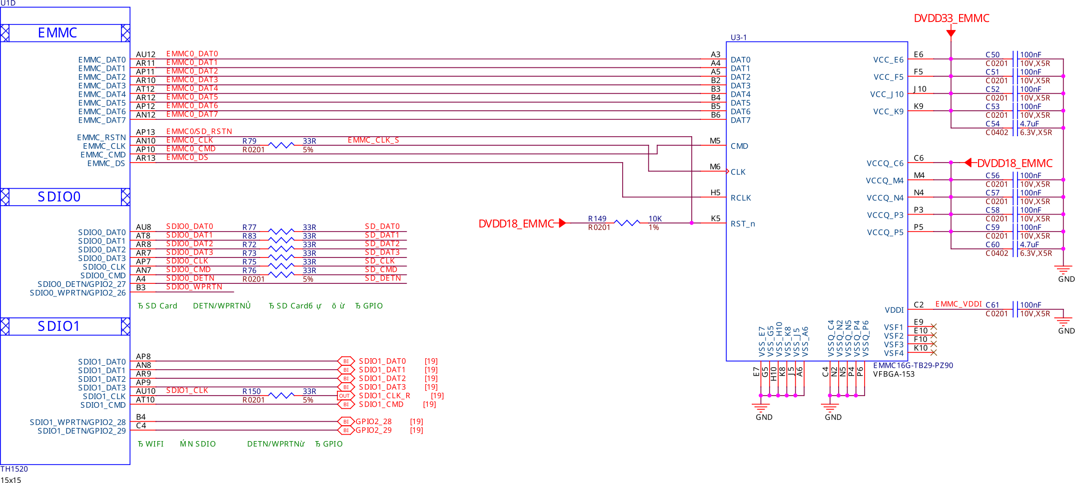
Fig. 217 16GB eMMC
microSD
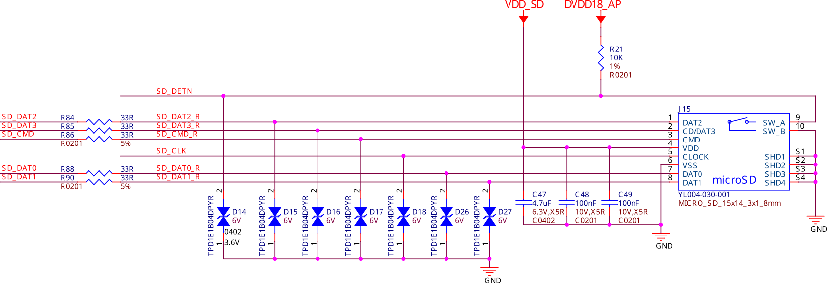
Fig. 218 microSD card connector
EEPROM
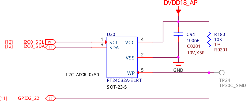
Fig. 219 16GB EEPROM
Multimedia I/O
CSI0
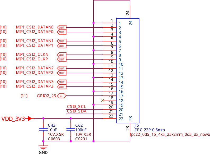
Fig. 220 CSI0 camera interface
CSI1
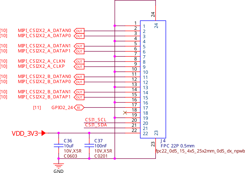
Fig. 221 CSI1 camera interface
DSI
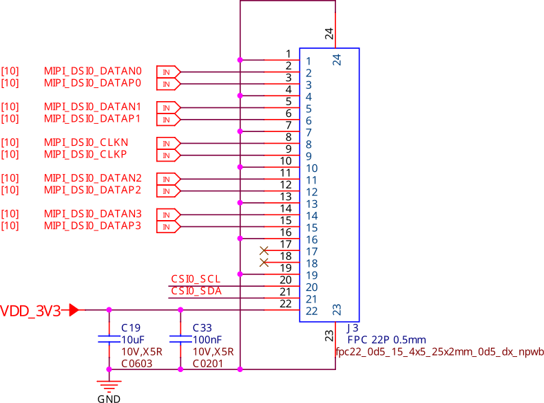
Fig. 222 DSI display interface
CSI & DSI level shifter
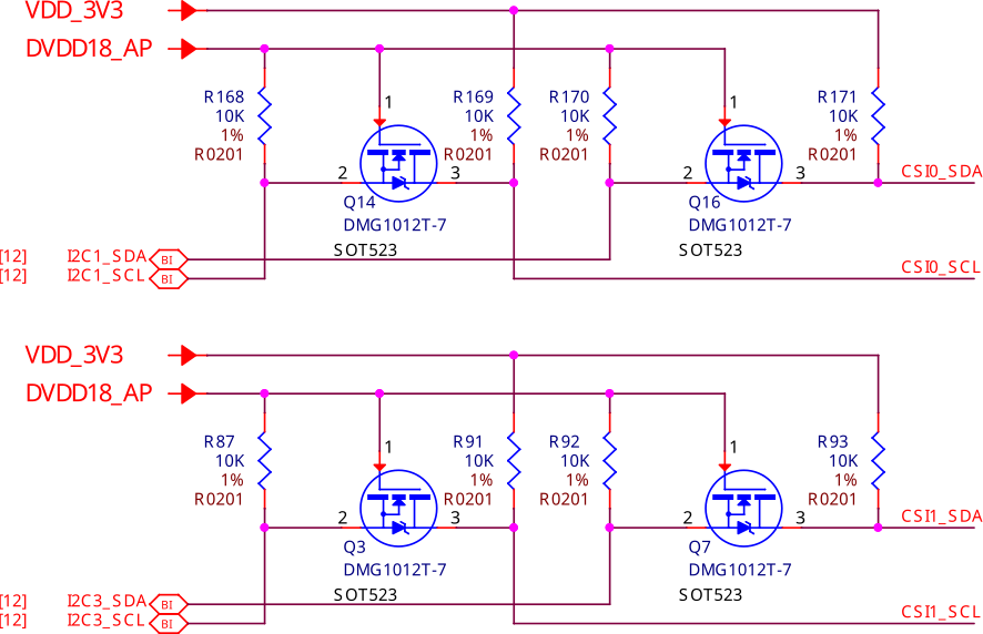
Fig. 223 CSI & DSI level shifter
HDMI
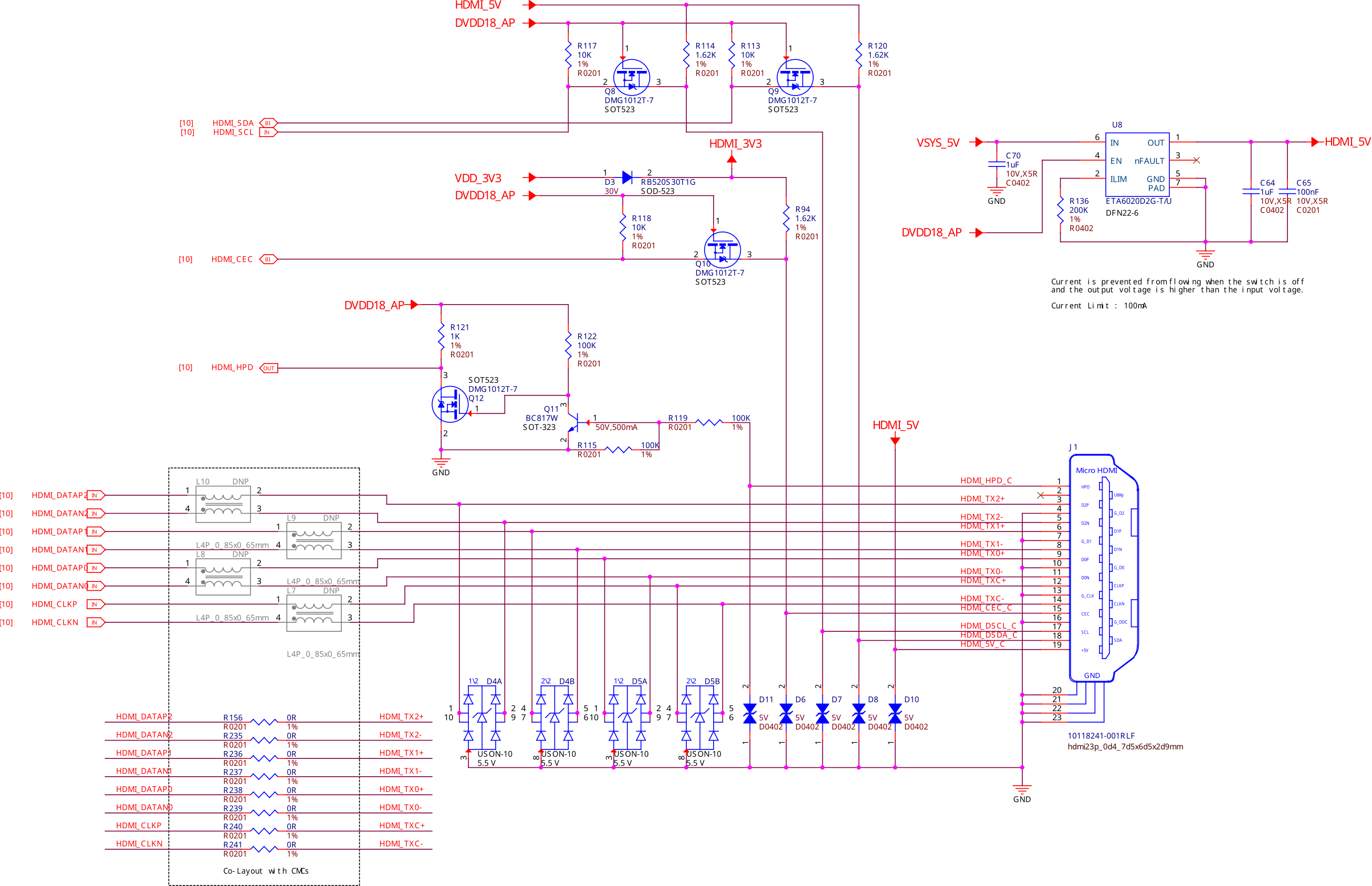
Fig. 224 HDMI display interface
Debug
UART debug port
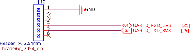
Fig. 225 UART Debug port
JTAG debug port
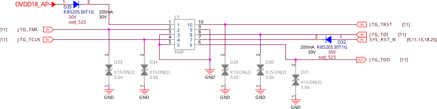
Fig. 226 JTAG debug port
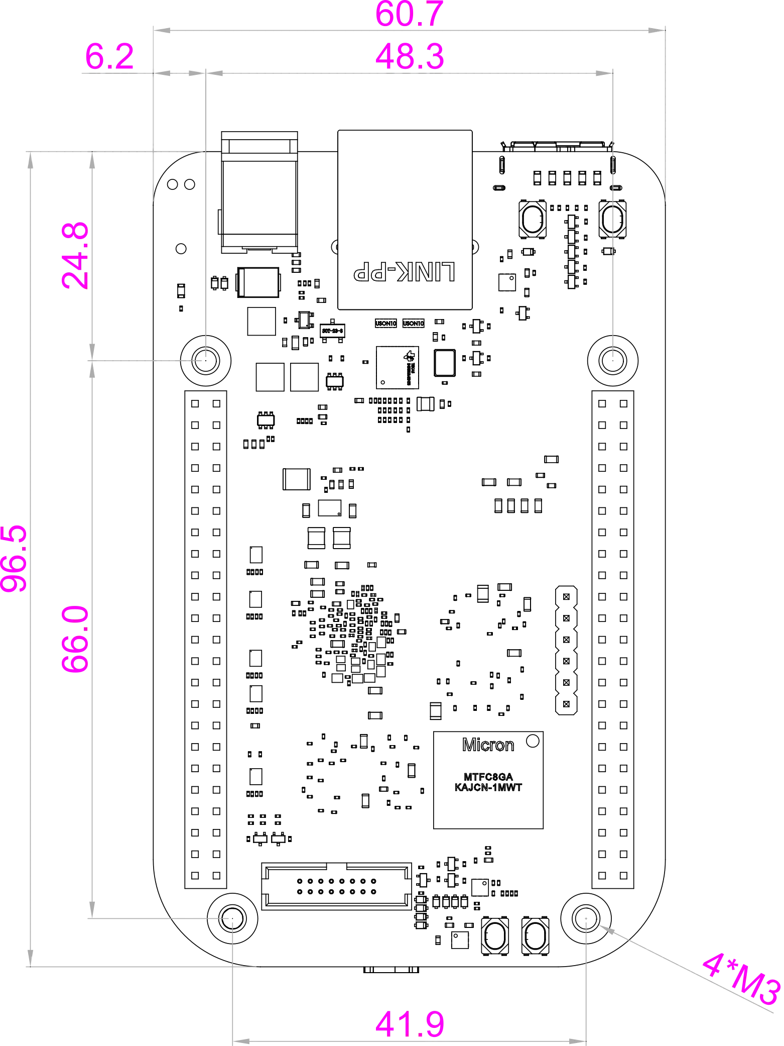
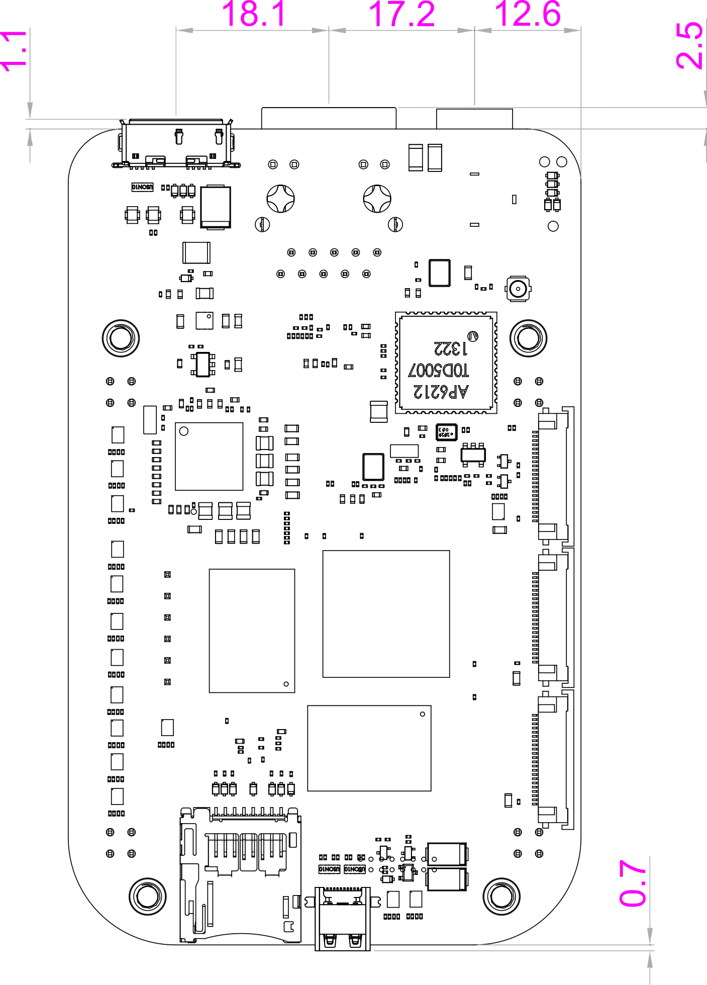
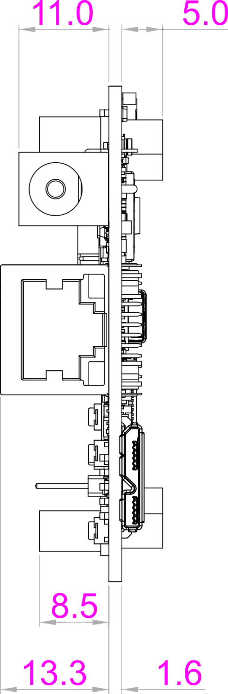
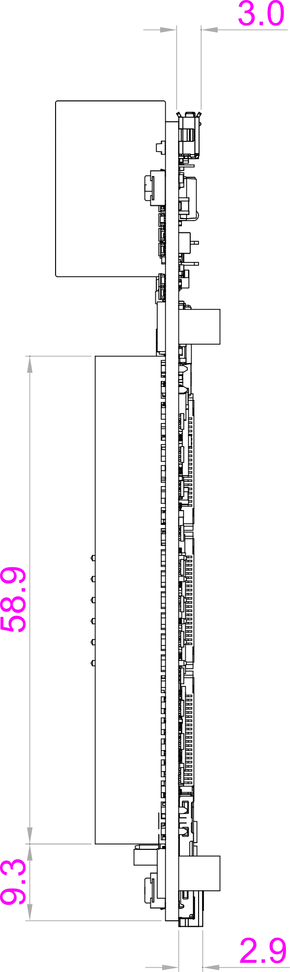
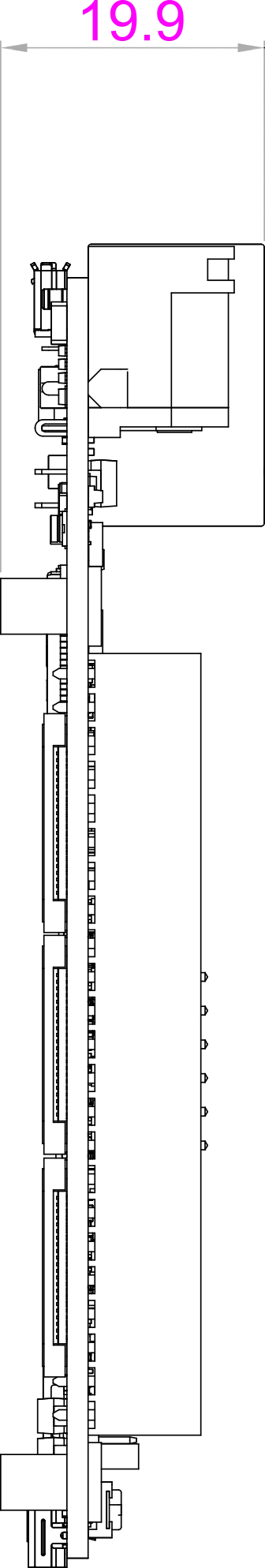
Mechanical Specifications
Top |
Bottom |
|---|---|
|
|
Front |
Left |
Right |
|---|---|---|
|
|
|
Parameter |
Values |
|---|---|
Size |
96.5×60.7×19.9mm |
Max heigh |
21.1mm |
PCB Size |
96.5x60.5*1.6mm |
PCB Layers |
10 layers |
PCB Thickness |
1.6mm |
RoHS compliant |
yes |
Gross Weight |
128.8g |
Net weight |
49.7g |